Home > Press > Dutch Company SolMateS sells first Piezoelectric Materials Deposition Machine PiezoFlare 1200 to SINTEF: SolMateS and SINTEF start close collaboration on PiezoMEMS development
 |
Abstract:
SolMateS has received an order from SINTEF (Oslo, Norway) for its PiezoFlare 1200 Pulsed Laser Deposition (PLD) system. The system is scheduled for delivery in January 2013 and will be used for deposition of Piezoelectric materials (PZT) for development and pre-production of next generation MEMS applications.
Dutch Company SolMateS sells first Piezoelectric Materials Deposition Machine PiezoFlare 1200 to SINTEF: SolMateS and SINTEF start close collaboration on PiezoMEMS development
Enschede, Netherlands | Posted on December 5th, 2012"We are very pleased with SINTEF as launching customer, this order comes with a close collaboration between SolMateS and SINTEF to optimize our machine and process in their development line for multiple new MEMS applications". commented Arjen Janssens. "The combination of our innovative tool and their expertise in PiezoMEMS development gives rise to a state-of-the-art PiezoMEMS centre in Europe".
####
About SolMateS BV
SolMateS is a fast growing and ambitious company with 20 employees, located at Science Park Twente, in Enschede, the Netherlands. A spin-off of MESA+ Institute of Nanotechnology. SolMateS has brought a lab scale technology (pulsed laser deposition) towards the production arena. This technology enables the deposition of new generation materials for the More than Moore applications, like Piezoelectric PZT. SolMateS has already been awarded with several technology and business awards since its launch in 2006. For more information, visit SolMateS' website at www.solmates.nl.
About SINTEF
SINTEF is the largest independent research organization in Scandinavia with over 2100 employees and annual sales of NOK 2,8 billion (380 million �). SINTEF is a multidisciplinary non-commercial organization with expertise in natural sciences and technology, environment, health and social science and provides contract research for Norwegian and international customers. SINTEF's ambition is to create value for customers through knowledge generation, research and innovation, and development of sustainable technological solutions. Operating profits are invested in new research, scientific equipment and competence development. For more information visit SINTEF's website at www.sintef.no. The department of Microsystems and Nanotechnology, SINTEF MiNaLab, provides services (R&D and small scale production) in silicon processing and device fabrication. By combining leading expertise in PZT material and processing technology, SINTEF has become a major player in Europe in the field of PiezoMEMS and PZT integration in MEMS. SINTEF aims at establishing a PiezoMEMS competence center to serve industry, promote the development of production processes and to develop innovative products.
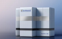
About the PiezoFlare 1200
The PiezoFlare 1200 is a revolutionary manufacturing technology to produce chips with precise actuation functionality for various new applications like, inkjet printheads, pico projectors, RF MEMS and various sensing applications. The PiezoFlare 1200 is an automated deposition system for PZT thin films on 6" or 8" wafers, based on pulsed laser deposition. The technology uses a laser to create a plasma of the to be deposited material, this has several significant advantages for the deposition of the new generation materials. The fully automated tool offers high-yield piezo performance and flexibility for customized PZT compositions and can also be used for other More than Moore materials.
For more information, please click here
Contacts:
Arjen Janssens
CEO
SolMateS
Tel. +31537009709
Fabrice Lapique
Research Director
SINTEF Microsystems and Nanotechnology
+4722067413.
Copyright © SolMateS BV
If you have a comment, please Contact us.Issuers of news releases, not 7th Wave, Inc. or Nanotechnology Now, are solely responsible for the accuracy of the content.
Bookmark:


| Related News Press |
News and information
![]() Simulating magnetization in a Heisenberg quantum spin chain April 5th, 2024
Simulating magnetization in a Heisenberg quantum spin chain April 5th, 2024
![]() NRL charters Navy�s quantum inertial navigation path to reduce drift April 5th, 2024
NRL charters Navy�s quantum inertial navigation path to reduce drift April 5th, 2024
![]() Discovery points path to flash-like memory for storing qubits: Rice find could hasten development of nonvolatile quantum memory April 5th, 2024
Discovery points path to flash-like memory for storing qubits: Rice find could hasten development of nonvolatile quantum memory April 5th, 2024
MEMS
Announcements
![]() NRL charters Navy�s quantum inertial navigation path to reduce drift April 5th, 2024
NRL charters Navy�s quantum inertial navigation path to reduce drift April 5th, 2024
![]() Discovery points path to flash-like memory for storing qubits: Rice find could hasten development of nonvolatile quantum memory April 5th, 2024
Discovery points path to flash-like memory for storing qubits: Rice find could hasten development of nonvolatile quantum memory April 5th, 2024
Tools
![]() Ferroelectrically modulate the Fermi level of graphene oxide to enhance SERS response November 3rd, 2023
Ferroelectrically modulate the Fermi level of graphene oxide to enhance SERS response November 3rd, 2023
![]() The USTC realizes In situ electron paramagnetic resonance spectroscopy using single nanodiamond sensors November 3rd, 2023
The USTC realizes In situ electron paramagnetic resonance spectroscopy using single nanodiamond sensors November 3rd, 2023
Battery Technology/Capacitors/Generators/Piezoelectrics/Thermoelectrics/Energy storage
![]() What heat can tell us about battery chemistry: using the Peltier effect to study lithium-ion cells March 8th, 2024
What heat can tell us about battery chemistry: using the Peltier effect to study lithium-ion cells March 8th, 2024
![]() A battery�s hopping ions remember where they�ve been: Seen in atomic detail, the seemingly smooth flow of ions through a battery�s electrolyte is surprisingly complicated February 16th, 2024
A battery�s hopping ions remember where they�ve been: Seen in atomic detail, the seemingly smooth flow of ions through a battery�s electrolyte is surprisingly complicated February 16th, 2024
|
|
||
|
|
||
| The latest news from around the world, FREE | ||
|
|
||
|
|
||
| Premium Products | ||
|
|
||
|
Only the news you want to read!
Learn More |
||
|
|
||
|
Full-service, expert consulting
Learn More |
||
|
|
||