Home > Press > Phenom-World is introducing Elemental Mapping for the PhenomTM proX desktop scanning electron microscope
 |
Abstract:
Elemental Mapping is the first expansion of the Phenom proX EDS-technology. The new 2.0 Element Identification (EID) software and the introduction of Elemental Mapping create a state of the art combination of hardware integration and dedicated software.
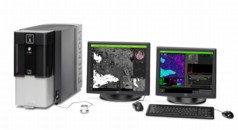
Phenom-World is introducing Elemental Mapping for the PhenomTM proX desktop scanning electron microscope
Eindhoven, The Netherlands | Posted on December 3rd, 2012-The introduction of the Elemental Mapping functionality for the Phenom proX desktop SEM opens up another information source. Where the standard EID generates information of individual spots on the sample, Elemental Mapping gives insight to the general distribution of the elements.
After the successful launch of the Phenom proX in March 2012, the first significant software update is now available. Besides the integration of the Elemental Mapping, the from Fibermetric renown step by step guided process is introduced into this software. This process guides the user to make all steps necessary to get the desired results. Whether a fast and efficient point analysis or a complex high detailed mapping is needed, it is a fast and easy job with the Phenom Elemental Identification software.
Smart mapping software options like real-time mapping algorithm show live build up of the selected element maps while storing spectra of each pixel. This allows adding or removing elements at any time during or after the mapping process. Mixing the mapped elements with the backscatter image gives users a phenomenal insight on the distribution of elements within the sample.
Elemental Mapping is an option available for any Phenom proX system. Visit our website www.phenom- world.com for application examples and a movie on Elemental Mapping and other EDS applications.
####
About Phenom-World
Phenom-World is a leading global supplier of desktop scanning electron microscopes and imaging and analysis packages for sub-micron-scale applications. Our SEM-based systems are used in a broad range of markets and environments. We continuously invest, develop, and integrate our products to help customers improve their return on investment, time to data, and to increase system functionality.
With representatives in more than 40 countries and a fast-growing installed base, we are committed to supporting our customers with our highly skilled team of specialists who provide application and service support on a global scale. We help our customers with excellent and fast results from the micro and nano world by supplying worry-free imaging and analysis.
Phenom-World BV is based in the high-tech region of Eindhoven in the Netherlands. This strategic position and collaboration with partners gives Phenom-World access to the newest technologies and best resources for developing state-of-the-art equipment and applications.
For more information, please click here
Contacts:
Dillenburgstraat 9E
5652 AM Eindhoven
The Netherlands
+31 (0)40 259 7360
Fax +31 (0)40 259 7370
Copyright © Phenom-World
If you have a comment, please Contact us.Issuers of news releases, not 7th Wave, Inc. or Nanotechnology Now, are solely responsible for the accuracy of the content.
Bookmark:


| Related News Press |
News and information
![]() Simulating magnetization in a Heisenberg quantum spin chain April 5th, 2024
Simulating magnetization in a Heisenberg quantum spin chain April 5th, 2024
![]() NRL charters Navy�s quantum inertial navigation path to reduce drift April 5th, 2024
NRL charters Navy�s quantum inertial navigation path to reduce drift April 5th, 2024
![]() Discovery points path to flash-like memory for storing qubits: Rice find could hasten development of nonvolatile quantum memory April 5th, 2024
Discovery points path to flash-like memory for storing qubits: Rice find could hasten development of nonvolatile quantum memory April 5th, 2024
Imaging
![]() Nanoscale CL thermometry with lanthanide-doped heavy-metal oxide in TEM March 8th, 2024
Nanoscale CL thermometry with lanthanide-doped heavy-metal oxide in TEM March 8th, 2024
![]() The USTC realizes In situ electron paramagnetic resonance spectroscopy using single nanodiamond sensors November 3rd, 2023
The USTC realizes In situ electron paramagnetic resonance spectroscopy using single nanodiamond sensors November 3rd, 2023
![]() Observation of left and right at nanoscale with optical force October 6th, 2023
Observation of left and right at nanoscale with optical force October 6th, 2023
Hardware
![]() The present and future of computing get a boost from new research July 21st, 2023
The present and future of computing get a boost from new research July 21st, 2023
Software
![]() Visualizing nanoscale structures in real time: Open-source software enables researchers to see materials in 3D while they're still on the electron microscope August 19th, 2022
Visualizing nanoscale structures in real time: Open-source software enables researchers to see materials in 3D while they're still on the electron microscope August 19th, 2022
![]() Luisier wins SNSF Advanced Grant to develop simulation tools for nanoscale devices July 8th, 2022
Luisier wins SNSF Advanced Grant to develop simulation tools for nanoscale devices July 8th, 2022
![]() Oxford Instruments� Atomfab� system is production-qualified at a market-leading GaN power electronics device manufacturer December 17th, 2021
Oxford Instruments� Atomfab� system is production-qualified at a market-leading GaN power electronics device manufacturer December 17th, 2021
Announcements
![]() NRL charters Navy�s quantum inertial navigation path to reduce drift April 5th, 2024
NRL charters Navy�s quantum inertial navigation path to reduce drift April 5th, 2024
![]() Discovery points path to flash-like memory for storing qubits: Rice find could hasten development of nonvolatile quantum memory April 5th, 2024
Discovery points path to flash-like memory for storing qubits: Rice find could hasten development of nonvolatile quantum memory April 5th, 2024
Tools
![]() Ferroelectrically modulate the Fermi level of graphene oxide to enhance SERS response November 3rd, 2023
Ferroelectrically modulate the Fermi level of graphene oxide to enhance SERS response November 3rd, 2023
![]() The USTC realizes In situ electron paramagnetic resonance spectroscopy using single nanodiamond sensors November 3rd, 2023
The USTC realizes In situ electron paramagnetic resonance spectroscopy using single nanodiamond sensors November 3rd, 2023
|
|
||
|
|
||
| The latest news from around the world, FREE | ||
|
|
||
|
|
||
| Premium Products | ||
|
|
||
|
Only the news you want to read!
Learn More |
||
|
|
||
|
Full-service, expert consulting
Learn More |
||
|
|
||