Home > Press > James’ bond: A graphene/nanotube hybrid
 |
Abstract:
A seamless graphene/nanotube hybrid created at Rice University may be the best electrode interface material possible for many energy storage and electronics applications.
James’ bond: A graphene/nanotube hybrid
Germany | Posted on November 29th, 2012Led by Rice chemist James Tour, researchers have successfully grown forests of carbon nanotubes that rise quickly from sheets of graphene to astounding lengths of up to 120 microns, according to newly published work. A house on an average plot with the same aspect ratio would rise into space.
That translates into a massive amount of surface area, the key factor in making things like energy-storing supercapacitors.
The Rice hybrid combines two-dimensional graphene, which is a sheet of carbon one atom thick, and nanotubes into a seamless three-dimensional structure. The bonds between them are covalent, which means adjacent carbon atoms share electrons in a highly stable configuration. The nanotubes aren't merely sitting on the graphene sheet; they become a part of it.
"Many people have tried to attach nanotubes to a metal electrode and it's never gone very well because they get a little electronic barrier right at the interface," Tour said. "By growing graphene on metal (in this case copper) and then growing nanotubes from the graphene, the electrical contact between the nanotubes and the metal electrode is ohmic. That means electrons see no difference, because it's all one seamless material.
"This gives us, effectively, a very high surface area of more than 2,000 square meters per gram of material. It's a huge number," said Tour, Rice's T.T. and W.F. Chao Chair in Chemistry as well as a professor of mechanical engineering and materials science and of computer science and a co-author with former postdoctoral researcher and lead author Yu Zhu, now an assistant professor at the University of Akron.
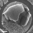
Tour said proof of the material's hybrid nature lies in the seven-membered rings at the transition from graphene to nanotube, a structure predicted by theory for such a material and now confirmed through electron microscope images with subnanometer resolution.
Carbon has no peer as a conductive material in such a thin and robust form, especially in the form of graphene or certain types of nanotubes. Combining the two appears to offer great potential for electronic components like fast supercapacitors that, because of the massive surface area, may hold a great deal of energy in a tiny package.
Rice chemist Robert Hauge and his team made the first steps toward such a hybrid over the past decade. Hauge, a distinguished faculty fellow in chemistry at Rice and co-author of the new work, discovered a way to make densely packed carpets of nanotubes on a carbon substrate by suspending catalyst-laced flakes in a furnace. When heated, the catalyst built carbon nanotubes like skyscrapers, starting at the substrate and working their way up. In the process, they lifted the aluminum oxide buffer into the air. The whole thing looked like a kite with many strings and was dubbed an odako, like the giant Japanese kites.
In the new work, the team grew a specialized odako that retained the iron catalyst and aluminum oxide buffer but put them on top of a layer of graphene grown separately on a copper substrate. The copper stayed to serve as an excellent current collector for the three-dimensional hybrids that were grown within minutes to controllable lengths of up to 120 microns.
Electron microscope images showed the one-, two- and three-walled nanotubes firmly embedded in the graphene, and electrical testing showed no resistance to the flow of current at the junction.
"The performance we see in this study is as good as the best carbon-based supercapacitors that have ever been made," Tour said. "We're not really a supercapacitor lab, and still we were able to match the performance because of the quality of the electrode. It's really remarkable, and it all harkens back to that unique interface."
####
For more information, please click here
Copyright © Wiley-VCH Materials Science Journals
If you have a comment, please Contact us.Issuers of news releases, not 7th Wave, Inc. or Nanotechnology Now, are solely responsible for the accuracy of the content.
Bookmark:


| Related Links |
| Related News Press |
News and information
![]() Simulating magnetization in a Heisenberg quantum spin chain April 5th, 2024
Simulating magnetization in a Heisenberg quantum spin chain April 5th, 2024
![]() NRL charters Navy’s quantum inertial navigation path to reduce drift April 5th, 2024
NRL charters Navy’s quantum inertial navigation path to reduce drift April 5th, 2024
![]() Discovery points path to flash-like memory for storing qubits: Rice find could hasten development of nonvolatile quantum memory April 5th, 2024
Discovery points path to flash-like memory for storing qubits: Rice find could hasten development of nonvolatile quantum memory April 5th, 2024
Graphene/ Graphite
![]() NRL discovers two-dimensional waveguides February 16th, 2024
NRL discovers two-dimensional waveguides February 16th, 2024
Chip Technology
![]() Discovery points path to flash-like memory for storing qubits: Rice find could hasten development of nonvolatile quantum memory April 5th, 2024
Discovery points path to flash-like memory for storing qubits: Rice find could hasten development of nonvolatile quantum memory April 5th, 2024
![]() Utilizing palladium for addressing contact issues of buried oxide thin film transistors April 5th, 2024
Utilizing palladium for addressing contact issues of buried oxide thin film transistors April 5th, 2024
![]() HKUST researchers develop new integration technique for efficient coupling of III-V and silicon February 16th, 2024
HKUST researchers develop new integration technique for efficient coupling of III-V and silicon February 16th, 2024
Discoveries
![]() Chemical reactions can scramble quantum information as well as black holes April 5th, 2024
Chemical reactions can scramble quantum information as well as black holes April 5th, 2024
![]() New micromaterial releases nanoparticles that selectively destroy cancer cells April 5th, 2024
New micromaterial releases nanoparticles that selectively destroy cancer cells April 5th, 2024
![]() Utilizing palladium for addressing contact issues of buried oxide thin film transistors April 5th, 2024
Utilizing palladium for addressing contact issues of buried oxide thin film transistors April 5th, 2024
Announcements
![]() NRL charters Navy’s quantum inertial navigation path to reduce drift April 5th, 2024
NRL charters Navy’s quantum inertial navigation path to reduce drift April 5th, 2024
![]() Discovery points path to flash-like memory for storing qubits: Rice find could hasten development of nonvolatile quantum memory April 5th, 2024
Discovery points path to flash-like memory for storing qubits: Rice find could hasten development of nonvolatile quantum memory April 5th, 2024
Energy
![]() Development of zinc oxide nanopagoda array photoelectrode: photoelectrochemical water-splitting hydrogen production January 12th, 2024
Development of zinc oxide nanopagoda array photoelectrode: photoelectrochemical water-splitting hydrogen production January 12th, 2024
![]() Shedding light on unique conduction mechanisms in a new type of perovskite oxide November 17th, 2023
Shedding light on unique conduction mechanisms in a new type of perovskite oxide November 17th, 2023
![]() Inverted perovskite solar cell breaks 25% efficiency record: Researchers improve cell efficiency using a combination of molecules to address different November 17th, 2023
Inverted perovskite solar cell breaks 25% efficiency record: Researchers improve cell efficiency using a combination of molecules to address different November 17th, 2023
![]() The efficient perovskite cells with a structured anti-reflective layer – another step towards commercialization on a wider scale October 6th, 2023
The efficient perovskite cells with a structured anti-reflective layer – another step towards commercialization on a wider scale October 6th, 2023
Battery Technology/Capacitors/Generators/Piezoelectrics/Thermoelectrics/Energy storage
![]() What heat can tell us about battery chemistry: using the Peltier effect to study lithium-ion cells March 8th, 2024
What heat can tell us about battery chemistry: using the Peltier effect to study lithium-ion cells March 8th, 2024
![]() A battery’s hopping ions remember where they’ve been: Seen in atomic detail, the seemingly smooth flow of ions through a battery’s electrolyte is surprisingly complicated February 16th, 2024
A battery’s hopping ions remember where they’ve been: Seen in atomic detail, the seemingly smooth flow of ions through a battery’s electrolyte is surprisingly complicated February 16th, 2024
|
|
||
|
|
||
| The latest news from around the world, FREE | ||
|
|
||
|
|
||
| Premium Products | ||
|
|
||
|
Only the news you want to read!
Learn More |
||
|
|
||
|
Full-service, expert consulting
Learn More |
||
|
|
||