Home > Press > Research discovery could revolutionize semiconductor manufacture
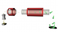 |
| Image: Aerotaxy production process |
Abstract:
A completely new method of manufacturing the smallest structures in electronics could make their manufacture thousands of times quicker, allowing for cheaper semiconductors. The findings have been published in the latest issue of Nature.
Instead of starting from a silicon wafer or other substrate, as is usual today, researchers have made it possible for the structures to grow from freely suspended nanoparticles of gold in a flowing gas.
Research discovery could revolutionize semiconductor manufacture
Lund, Sweden | Posted on November 29th, 2012 Behind the discovery is Lars Samuelson, Professor of Semiconductor Physics at Lund University, Sweden, and head of the University's Nanometre Structure Consortium. He believes the technology will be ready for commercialisation in two to four years' time. A prototype for solar cells is expected to be completed in two years.
"When I first suggested the idea of getting rid of the substrate, people around me said �you're out of your mind, Lars; that would never work'. When we tested the principle in one of our converted ovens at 400�C, the results were better than we could have dreamt of", he says.
"The basic idea was to let nanoparticles of gold serve as a substrate from which the semiconductors grow. This means that the accepted concepts really were turned upside down!"
Since then, the technology has been refined, patents have been obtained and further studies have been conducted. In the article in Nature, the researchers show how the growth can be controlled using temperature, time and the size of the gold nanoparticles.
Recently, they have also built a prototype machine with a specially built oven. Using a series of ovens, the researchers expect to be able to �bake' the nanowires, as the structures are called, and thereby develop multiple variants, such as p-n diodes.
A further advantage of the technology is avoiding the cost of expensive semiconductor wafers.
"In addition, the process is not only extremely quick, it is also continuous. Traditional manufacture of substrates is batch-based and is therefore much more time-consuming", adds Lars Samuelson.
At the moment, the researchers are working to develop a good method to capture the nanowires and make them self-assemble in an ordered manner on a specific surface. This could be glass, steel or another material suited to the purpose.
The reason why no one has tested this method before, in the view of Professor Samuelson, is that today's method is so basic and obvious. Such things tend to be difficult to question.
However, the Lund researchers have a head start thanks to their parallel research based on an innovative method in the manufacture of nanowires on semiconductor wafers, known as epitaxy - consequently, the researchers have chosen to call the new method aerotaxy. Instead of sculpting structures out of silicon or another semiconductor material, the structures are instead allowed to develop, atomic layer by atomic layer, through controlled self-organisation.
The structures are referred to as nanowires or nanorods. The breakthrough for these semiconductor structures came in 2002 and research on them is primarily carried out at Lund, Berkeley and Harvard universities.
The Lund researchers specialise in developing the physical and electrical properties of the wires, which helps create better and more energy-saving solar cells, LEDs, batteries and other electrical equipment that is now an integrated part of our lives.
The article �Continuous gas-phase synthesis of nanowires with tuneable properties' can be found by entering "I 10.1038/nature11652" here: http://dx.doi.org/.
Besides Lars Samuelson, the other authors of the article are: Magnus Heurlin, Martin Magnusson, David Lindgren, Martin Ek, Reine Wallenberg and Knut Deppert, all employed at Lund University, except for Martin Magnusson, who works at start-up company Sol Voltaics AB.
The research has been funded by the Swedish Research Council, the Swedish Foundation for Strategic Research (SSF), the Knut and Alice Wallenberg Foundation and Vinnova.
####
About Lund University
Lund University seeks to be a world-class university that works to understand, explain and improve our world and the human condition. The University is ranked as one of the top 100 in the world. We tackle complex problems and global challenges and work to ensure that knowledge and innovations benefit society. We provide education and research in engineering, science, law, social sciences, economics and management, medicine, humanities, theology, fine art, music and drama.
Our 47 000 students and 6 800 employees are based at our campuses in Lund, Malm� and Helsingborg. The University has a turnover of around EUR 700 million (or USD 900 million), of which two thirds is in research and one third in education.
About semiconductors
Semiconductors are materials that neither conduct electricity as well as metals, nor stop a current as effectively as insulators � silicon and germanium are two examples. These properties may not sound attractive, but in actual fact they are excellent. The reason is that we can influence the conductive capacity of the materials, for example by introducing impurity atoms, known as doping. Materials with different types of doping can be combined to manufacture products such as transistors, solar cells or LEDs.
For more information, please click here
Contacts:
Lars Samuelson
+46 46 222 76 79
+46-703-177-679
Copyright © Lund University
If you have a comment, please Contact us.Issuers of news releases, not 7th Wave, Inc. or Nanotechnology Now, are solely responsible for the accuracy of the content.
Bookmark:


| Related Links |
![]() Contact details for the other authors can be found by searching on www.lunduniversity.lu.se:
Contact details for the other authors can be found by searching on www.lunduniversity.lu.se:
![]() Lund University Nanometre Structure Consortium, nmC@LU:
Lund University Nanometre Structure Consortium, nmC@LU:
| Related News Press |
News and information
![]() Simulating magnetization in a Heisenberg quantum spin chain April 5th, 2024
Simulating magnetization in a Heisenberg quantum spin chain April 5th, 2024
![]() NRL charters Navy�s quantum inertial navigation path to reduce drift April 5th, 2024
NRL charters Navy�s quantum inertial navigation path to reduce drift April 5th, 2024
![]() Discovery points path to flash-like memory for storing qubits: Rice find could hasten development of nonvolatile quantum memory April 5th, 2024
Discovery points path to flash-like memory for storing qubits: Rice find could hasten development of nonvolatile quantum memory April 5th, 2024
Govt.-Legislation/Regulation/Funding/Policy
![]() NRL charters Navy�s quantum inertial navigation path to reduce drift April 5th, 2024
NRL charters Navy�s quantum inertial navigation path to reduce drift April 5th, 2024
![]() Discovery points path to flash-like memory for storing qubits: Rice find could hasten development of nonvolatile quantum memory April 5th, 2024
Discovery points path to flash-like memory for storing qubits: Rice find could hasten development of nonvolatile quantum memory April 5th, 2024
![]() Chemical reactions can scramble quantum information as well as black holes April 5th, 2024
Chemical reactions can scramble quantum information as well as black holes April 5th, 2024
Chip Technology
![]() Discovery points path to flash-like memory for storing qubits: Rice find could hasten development of nonvolatile quantum memory April 5th, 2024
Discovery points path to flash-like memory for storing qubits: Rice find could hasten development of nonvolatile quantum memory April 5th, 2024
![]() Utilizing palladium for addressing contact issues of buried oxide thin film transistors April 5th, 2024
Utilizing palladium for addressing contact issues of buried oxide thin film transistors April 5th, 2024
![]() HKUST researchers develop new integration technique for efficient coupling of III-V and silicon February 16th, 2024
HKUST researchers develop new integration technique for efficient coupling of III-V and silicon February 16th, 2024
Discoveries
![]() Chemical reactions can scramble quantum information as well as black holes April 5th, 2024
Chemical reactions can scramble quantum information as well as black holes April 5th, 2024
![]() New micromaterial releases nanoparticles that selectively destroy cancer cells April 5th, 2024
New micromaterial releases nanoparticles that selectively destroy cancer cells April 5th, 2024
![]() Utilizing palladium for addressing contact issues of buried oxide thin film transistors April 5th, 2024
Utilizing palladium for addressing contact issues of buried oxide thin film transistors April 5th, 2024
Announcements
![]() NRL charters Navy�s quantum inertial navigation path to reduce drift April 5th, 2024
NRL charters Navy�s quantum inertial navigation path to reduce drift April 5th, 2024
![]() Discovery points path to flash-like memory for storing qubits: Rice find could hasten development of nonvolatile quantum memory April 5th, 2024
Discovery points path to flash-like memory for storing qubits: Rice find could hasten development of nonvolatile quantum memory April 5th, 2024
Energy
![]() Development of zinc oxide nanopagoda array photoelectrode: photoelectrochemical water-splitting hydrogen production January 12th, 2024
Development of zinc oxide nanopagoda array photoelectrode: photoelectrochemical water-splitting hydrogen production January 12th, 2024
![]() Shedding light on unique conduction mechanisms in a new type of perovskite oxide November 17th, 2023
Shedding light on unique conduction mechanisms in a new type of perovskite oxide November 17th, 2023
![]() Inverted perovskite solar cell breaks 25% efficiency record: Researchers improve cell efficiency using a combination of molecules to address different November 17th, 2023
Inverted perovskite solar cell breaks 25% efficiency record: Researchers improve cell efficiency using a combination of molecules to address different November 17th, 2023
![]() The efficient perovskite cells with a structured anti-reflective layer � another step towards commercialization on a wider scale October 6th, 2023
The efficient perovskite cells with a structured anti-reflective layer � another step towards commercialization on a wider scale October 6th, 2023
Solar/Photovoltaic
![]() Development of zinc oxide nanopagoda array photoelectrode: photoelectrochemical water-splitting hydrogen production January 12th, 2024
Development of zinc oxide nanopagoda array photoelectrode: photoelectrochemical water-splitting hydrogen production January 12th, 2024
![]() Shedding light on unique conduction mechanisms in a new type of perovskite oxide November 17th, 2023
Shedding light on unique conduction mechanisms in a new type of perovskite oxide November 17th, 2023
![]() Inverted perovskite solar cell breaks 25% efficiency record: Researchers improve cell efficiency using a combination of molecules to address different November 17th, 2023
Inverted perovskite solar cell breaks 25% efficiency record: Researchers improve cell efficiency using a combination of molecules to address different November 17th, 2023
![]() Charged �molecular beasts� the basis for new compounds: Researchers at Leipzig University use �aggressive� fragments of molecular ions for chemical synthesis November 3rd, 2023
Charged �molecular beasts� the basis for new compounds: Researchers at Leipzig University use �aggressive� fragments of molecular ions for chemical synthesis November 3rd, 2023
|
|
||
|
|
||
| The latest news from around the world, FREE | ||
|
|
||
|
|
||
| Premium Products | ||
|
|
||
|
Only the news you want to read!
Learn More |
||
|
|
||
|
Full-service, expert consulting
Learn More |
||
|
|
||