Home > Press > ORNL pushes the boundaries of electron microscopy to unlock the potential of graphene
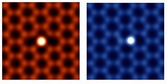 |
| The atomic resolution Z-contrast images show individual silicon atoms bonded differently in graphene. |
Abstract:
Electron microscopy at the Department of Energy's Oak Ridge National Laboratory is providing unprecedented views of the individual atoms in graphene, offering scientists a chance to unlock the material's full potential for uses from engine combustion to consumer electronics.
ORNL pushes the boundaries of electron microscopy to unlock the potential of graphene
Oak Ridge, TN | Posted on November 16th, 2012 Graphene crystals were first isolated in 2004. They are two-dimensional (one-atom in thickness), harder than diamonds and far stronger than steel, providing unprecedented stiffness, electrical and thermal properties. By viewing the atomic and bonding configurations of individual graphene atoms, scientists are able to suggest ways to optimize materials so they are better suited for specific applications.
In a paper published in Physical Review Letters, a team of researchers from Oak Ridge National Laboratory and Vanderbilt University used aberration-corrected scanning transmission electron microscopy to study the atomic and electronic structure of silicon impurities in graphene.
"We have used new experimental and computational tools to reveal the bonding characteristics of individual impurities in graphene. For instance, we can now differentiate between a non-carbon atom that is two-dimensionally or three-dimensionally bonded in graphene. In fact, we were finally able to directly visualize a bonding configuration that was predicted in the 1930s but has never been observed experimentally," said ORNL researcher Juan-Carlos Idrobo. Electrons in orbit around an atom fall into four broad categories - s, p, d and f - based on factors including symmetry and energy levels.
"We observed that silicon d-states participate in the bonding only when the silicon is two-dimensionally coordinated," Idrobo said. "There are many elements such as chromium, iron, and copper where the d-states or d-electrons play a dominant role in determining how the element bonds in a material."
By studying the atomic and electronic structure of graphene and identifying any impurities, researchers can better predict which elemental additions will improve the material's performance.
Slightly altering the chemical makeup of graphene could customize the material, making it more suitable for a variety of applications. For example, one elemental addition may make the material a better replacement for the platinum catalytic converters in cars, while another may allow it to function better in electronic devices or as a membrane.
Graphene has the potential to replace the inner workings of electronic gadgets people use every day because of its ability to conduct heat and electricity and its optical transparency. It offers a cheaper and more abundant alternative to indium, a limited resource that is widely used in the transparent conducting coating present in almost all electronic display devices such as digital displays in cars, TVs, laptops and handheld gadgets like cell phones, tablets and music players.
Researchers expect the imaging techniques demonstrated at ORNL to be used to understand the atomic structures and bonding characteristics of atoms in other two-dimensional materials, too.
The authors of the paper are Wu Zhou, Myron Kapetanakis, Micah Prange, Sokrates Pantelides, Stephen Pennycook and Idrobo.
This research was supported by National Science Foundation and the DOE Office of Science. Researchers also made use of Oak Ridge National Laboratory's Shared Research Equipment User Facility along with Lawrence Berkeley National Laboratory's National Energy Research Scientific Computing Center, both of which are also supported by DOE's Office of Science.
####
About DOE/Oak Ridge National Laboratory
ORNL is managed by UT-Battelle for the Department of Energy's Office of Science. DOE's Office of Science is the single largest supporter of basic research in the physical sciences in the United States, and is working to address some of the most pressing challenges of our time. For more information, please visit science.energy.gov.
For more information, please click here
Contacts:
Jennifer Brouner
865-241-9515
Copyright © DOE/Oak Ridge National Laboratory
If you have a comment, please Contact us.Issuers of news releases, not 7th Wave, Inc. or Nanotechnology Now, are solely responsible for the accuracy of the content.
Bookmark:


| Related News Press |
News and information
![]() Simulating magnetization in a Heisenberg quantum spin chain April 5th, 2024
Simulating magnetization in a Heisenberg quantum spin chain April 5th, 2024
![]() NRL charters Navy�s quantum inertial navigation path to reduce drift April 5th, 2024
NRL charters Navy�s quantum inertial navigation path to reduce drift April 5th, 2024
![]() Discovery points path to flash-like memory for storing qubits: Rice find could hasten development of nonvolatile quantum memory April 5th, 2024
Discovery points path to flash-like memory for storing qubits: Rice find could hasten development of nonvolatile quantum memory April 5th, 2024
![]() Good as gold - improving infectious disease testing with gold nanoparticles April 5th, 2024
Good as gold - improving infectious disease testing with gold nanoparticles April 5th, 2024
Display technology/LEDs/SS Lighting/OLEDs
![]() Utilizing palladium for addressing contact issues of buried oxide thin film transistors April 5th, 2024
Utilizing palladium for addressing contact issues of buried oxide thin film transistors April 5th, 2024
Graphene/ Graphite
![]() NRL discovers two-dimensional waveguides February 16th, 2024
NRL discovers two-dimensional waveguides February 16th, 2024
Laboratories
![]() A battery�s hopping ions remember where they�ve been: Seen in atomic detail, the seemingly smooth flow of ions through a battery�s electrolyte is surprisingly complicated February 16th, 2024
A battery�s hopping ions remember where they�ve been: Seen in atomic detail, the seemingly smooth flow of ions through a battery�s electrolyte is surprisingly complicated February 16th, 2024
![]() NRL discovers two-dimensional waveguides February 16th, 2024
NRL discovers two-dimensional waveguides February 16th, 2024
Govt.-Legislation/Regulation/Funding/Policy
![]() NRL charters Navy�s quantum inertial navigation path to reduce drift April 5th, 2024
NRL charters Navy�s quantum inertial navigation path to reduce drift April 5th, 2024
![]() Discovery points path to flash-like memory for storing qubits: Rice find could hasten development of nonvolatile quantum memory April 5th, 2024
Discovery points path to flash-like memory for storing qubits: Rice find could hasten development of nonvolatile quantum memory April 5th, 2024
![]() Chemical reactions can scramble quantum information as well as black holes April 5th, 2024
Chemical reactions can scramble quantum information as well as black holes April 5th, 2024
Chip Technology
![]() Discovery points path to flash-like memory for storing qubits: Rice find could hasten development of nonvolatile quantum memory April 5th, 2024
Discovery points path to flash-like memory for storing qubits: Rice find could hasten development of nonvolatile quantum memory April 5th, 2024
![]() Utilizing palladium for addressing contact issues of buried oxide thin film transistors April 5th, 2024
Utilizing palladium for addressing contact issues of buried oxide thin film transistors April 5th, 2024
![]() HKUST researchers develop new integration technique for efficient coupling of III-V and silicon February 16th, 2024
HKUST researchers develop new integration technique for efficient coupling of III-V and silicon February 16th, 2024
Discoveries
![]() Chemical reactions can scramble quantum information as well as black holes April 5th, 2024
Chemical reactions can scramble quantum information as well as black holes April 5th, 2024
![]() New micromaterial releases nanoparticles that selectively destroy cancer cells April 5th, 2024
New micromaterial releases nanoparticles that selectively destroy cancer cells April 5th, 2024
![]() Utilizing palladium for addressing contact issues of buried oxide thin film transistors April 5th, 2024
Utilizing palladium for addressing contact issues of buried oxide thin film transistors April 5th, 2024
Materials/Metamaterials/Magnetoresistance
![]() Nanoscale CL thermometry with lanthanide-doped heavy-metal oxide in TEM March 8th, 2024
Nanoscale CL thermometry with lanthanide-doped heavy-metal oxide in TEM March 8th, 2024
![]() Focused ion beam technology: A single tool for a wide range of applications January 12th, 2024
Focused ion beam technology: A single tool for a wide range of applications January 12th, 2024
Announcements
![]() NRL charters Navy�s quantum inertial navigation path to reduce drift April 5th, 2024
NRL charters Navy�s quantum inertial navigation path to reduce drift April 5th, 2024
![]() Discovery points path to flash-like memory for storing qubits: Rice find could hasten development of nonvolatile quantum memory April 5th, 2024
Discovery points path to flash-like memory for storing qubits: Rice find could hasten development of nonvolatile quantum memory April 5th, 2024
Automotive/Transportation
![]() Researchers� approach may protect quantum computers from attacks March 8th, 2024
Researchers� approach may protect quantum computers from attacks March 8th, 2024
![]() Tests find no free-standing nanotubes released from tire tread wear September 8th, 2023
Tests find no free-standing nanotubes released from tire tread wear September 8th, 2023
|
|
||
|
|
||
| The latest news from around the world, FREE | ||
|
|
||
|
|
||
| Premium Products | ||
|
|
||
|
Only the news you want to read!
Learn More |
||
|
|
||
|
Full-service, expert consulting
Learn More |
||
|
|
||