Home > Press > Electron 'sniper' targets graphene
 |
Abstract:
Because of its intriguing properties graphene could be the ideal material for building new kinds of electronic devices such as sensors, screens, or even quantum computers.
Electron 'sniper' targets graphene
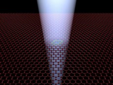
Oxford, UK | Posted on October 25th, 2012One of the keys to exploiting graphene's potential is being able to create atomic-scale defects - where carbon atoms in its flat, honeycomb-like structure are rearranged or 'knocked out' - as these influence its electrical, chemical, magnetic, and mechanical properties.
A team led by Oxford University scientists report in Nature Communications a new approach to a new approach to engineering graphene's atomic structure with unprecedented precision.
'Current approaches for producing defects in graphene are either like a 'shotgun' where the entire sample is sprayed with high energy ions or electrons to cause widespread defects, or a chemistry approach where many regions of the graphene are chemically reacted,' said Jamie Warner from Oxford University's Department of Materials, a member of the team.
'Both methods lack any form of control in terms of spatial precision and also the defect type, but to date are the only reported methods known for defect creation.'
The new method replaces the 'shotgun' with something more like a sniper rifle: a minutely-controlled beam of electrons fired from an electron microscope.
'The shotgun approach is restricted to micron scale precision, which is roughly an area of 10,000,000 square nanometres, we demonstrated a precision to within 100 square nanometres, which is about four orders of magnitude better,' explains Alex Robertson of Oxford University's Department of Materials, another member of the team.
Yet it isn't just about the accuracy of a single 'shot'; the researchers also show that by controlling the length of time graphene is exposed to their focused beam of electrons they can control the size and type of defect created.
'Our study reveals for the first time that only a few types of defects are actually stable in graphene, with several defects being quenched by surface atoms or relaxing back to pristine by bond rotations,' Jamie tells me.
The ability to create just the right kind of stable defects in graphene's crystal structure is going to be vital if its properties are to be harnessed for applications such as mobile phones and flexible displays.
'Defect sites in graphene are much more chemically reactive, so we can use defects as a site for chemical functionalisation of the graphene. So we can attach certain molecules, such as biomolecules, to the graphene to act as a sensor,' Alex tells me.
'Defects in graphene can also give rise to localized electron spin, an attribute that has important future use in quantum nanotechnology and quantum computers.'
At the moment scaling up the team's technique into a manufacturing process to create graphene-based technologies is still a way off. Currently electron microscopes are the only systems that can achieve the necessary exquisite control of an electron beam.
But, Alex says, it is always possible that a scalable electron beam lithography type technique may be developed in the future that could allow for defect patterning in graphene.
And it's worth remembering that it wasn't so long ago that the technology needed to etch millions of transistors onto a tiny slice of silicon seemed like an impossible dream.
####
About University of Oxford
Oxford is the oldest university in the English-speaking world, and a leader in learning, teaching and research.
For more information, please click here
Contacts:
Press & Information Office
telephone:+44 01865 280528
Copyright © University of Oxford
If you have a comment, please Contact us.Issuers of news releases, not 7th Wave, Inc. or Nanotechnology Now, are solely responsible for the accuracy of the content.
Bookmark:


| Related Links |
| Related News Press |
News and information
![]() Simulating magnetization in a Heisenberg quantum spin chain April 5th, 2024
Simulating magnetization in a Heisenberg quantum spin chain April 5th, 2024
![]() NRL charters Navy�s quantum inertial navigation path to reduce drift April 5th, 2024
NRL charters Navy�s quantum inertial navigation path to reduce drift April 5th, 2024
![]() Discovery points path to flash-like memory for storing qubits: Rice find could hasten development of nonvolatile quantum memory April 5th, 2024
Discovery points path to flash-like memory for storing qubits: Rice find could hasten development of nonvolatile quantum memory April 5th, 2024
![]() Good as gold - improving infectious disease testing with gold nanoparticles April 5th, 2024
Good as gold - improving infectious disease testing with gold nanoparticles April 5th, 2024
Display technology/LEDs/SS Lighting/OLEDs
![]() Utilizing palladium for addressing contact issues of buried oxide thin film transistors April 5th, 2024
Utilizing palladium for addressing contact issues of buried oxide thin film transistors April 5th, 2024
Graphene/ Graphite
![]() NRL discovers two-dimensional waveguides February 16th, 2024
NRL discovers two-dimensional waveguides February 16th, 2024
Quantum Computing
![]() Simulating magnetization in a Heisenberg quantum spin chain April 5th, 2024
Simulating magnetization in a Heisenberg quantum spin chain April 5th, 2024
![]() Discovery points path to flash-like memory for storing qubits: Rice find could hasten development of nonvolatile quantum memory April 5th, 2024
Discovery points path to flash-like memory for storing qubits: Rice find could hasten development of nonvolatile quantum memory April 5th, 2024
![]() With VECSELs towards the quantum internet Fraunhofer: IAF achieves record output power with VECSEL for quantum frequency converters April 5th, 2024
With VECSELs towards the quantum internet Fraunhofer: IAF achieves record output power with VECSEL for quantum frequency converters April 5th, 2024
![]() Chemical reactions can scramble quantum information as well as black holes April 5th, 2024
Chemical reactions can scramble quantum information as well as black holes April 5th, 2024
Sensors
Discoveries
![]() Chemical reactions can scramble quantum information as well as black holes April 5th, 2024
Chemical reactions can scramble quantum information as well as black holes April 5th, 2024
![]() New micromaterial releases nanoparticles that selectively destroy cancer cells April 5th, 2024
New micromaterial releases nanoparticles that selectively destroy cancer cells April 5th, 2024
![]() Utilizing palladium for addressing contact issues of buried oxide thin film transistors April 5th, 2024
Utilizing palladium for addressing contact issues of buried oxide thin film transistors April 5th, 2024
Announcements
![]() NRL charters Navy�s quantum inertial navigation path to reduce drift April 5th, 2024
NRL charters Navy�s quantum inertial navigation path to reduce drift April 5th, 2024
![]() Discovery points path to flash-like memory for storing qubits: Rice find could hasten development of nonvolatile quantum memory April 5th, 2024
Discovery points path to flash-like memory for storing qubits: Rice find could hasten development of nonvolatile quantum memory April 5th, 2024
Tools
![]() Ferroelectrically modulate the Fermi level of graphene oxide to enhance SERS response November 3rd, 2023
Ferroelectrically modulate the Fermi level of graphene oxide to enhance SERS response November 3rd, 2023
![]() The USTC realizes In situ electron paramagnetic resonance spectroscopy using single nanodiamond sensors November 3rd, 2023
The USTC realizes In situ electron paramagnetic resonance spectroscopy using single nanodiamond sensors November 3rd, 2023
Printing/Lithography/Inkjet/Inks/Bio-printing/Dyes
![]() Presenting: Ultrasound-based printing of 3D materials�potentially inside the body December 8th, 2023
Presenting: Ultrasound-based printing of 3D materials�potentially inside the body December 8th, 2023
![]() Simple ballpoint pen can write custom LEDs August 11th, 2023
Simple ballpoint pen can write custom LEDs August 11th, 2023
![]() Disposable electronics on a simple sheet of paper October 7th, 2022
Disposable electronics on a simple sheet of paper October 7th, 2022
|
|
||
|
|
||
| The latest news from around the world, FREE | ||
|
|
||
|
|
||
| Premium Products | ||
|
|
||
|
Only the news you want to read!
Learn More |
||
|
|
||
|
Full-service, expert consulting
Learn More |
||
|
|
||