Home > Press > Advanced Origami: Nanostructures From Flowers to Boxes
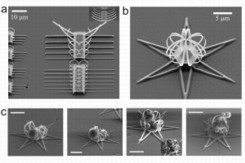 |
| Scanning electron microscopic (SEM) images: a) Self-rolling strips of different widths; b) metallic microflower; c) trapped microparticles of lactose in self-organized metallic structures (scale bar is 4 μm). |
Abstract:
Self-organising complex 3D structures on the nanometer scale hold tremendous promise in wide-ranging nanotechnological devices with important optical and biological applications. One of the key challenges facing researchers, however, lies in developing a fabrication process with extremely high precision, control, and reproducibility.
Advanced Origami: Nanostructures From Flowers to Boxes
Germany | Posted on October 11th, 2012A team from the Aalto University in Finland in collaboration with the University of Washington has made an important breakthrough utilising a phenomena that can be commonly observed outside the laboratory in the natural world, from the curling of flowers to the opening of seed capsules in ice plants: deformation through stress-relaxation. As reported in Advanced Materials, the researchers (K. Chalapat, N. Chekurov, H. Jiang, J. Li, B. Parviz and G. S. Paraoanu) from Aalto University have demonstrated how two different techniques, namely, reactive ion etching and focused ion beam, can be used to induce stress at defined locations on very nanometer-sized polycrystalline metal films, ultimately enabling them to manipulate the films into the desired complex 3D geometries.
Reactive ion etching, a technique commonly used for cleaning silicon wafers, involves exposure to a low-pressure plasma, in which high-energy ions collide and react with the substrate. When this technique is applied to thin strips of metal film on silicon wafer, this results in the insertion of adatoms into grain boundaries within the metal matrix. This induces a compressive stress, which, upon relaxing of the film, causes it to bend (see the figure to the left and the video at the bottom of the page). Interestingly, the extent of bending (radius of curvature) was found to be dependent on the width of the metal, thus permitting control over the final 3D geometry. Exploiting this concept, the team demonstrated a functional microscopic metallic flower-like structure (see below), with the capacity to trap microparticles (as a proof-of-concept, lactose particle were employed).
Using the more well-known process for fabricating defined nanometer-sized structures, focused ion beam (FIB), which involves bombarding the substrate with a beam of gallium ions, the researchers found that nanometallic cantilevers bent strongly toward the incident direction of the ion beam, effectively due to the compressive stress that results from atomic displacement. Moreover, a theoretical treatment showed that for a given material, the amount of bending is exclusively determined by the fluence of beam, meaning that by controlling the strength of the ion source, one can manipulate materials on the nanometer scale with extremely high precision and control. A remarkable example of this in practice is the fabrication of a nanobox (see video).The remarkable precision and control afforded by the novel methods reported here represents an important nanoengineering advance with far-reaching and exciting future applications.
####
For more information, please click here
Copyright © Wiley-VCH Materials Science Journals
If you have a comment, please Contact us.Issuers of news releases, not 7th Wave, Inc. or Nanotechnology Now, are solely responsible for the accuracy of the content.
Bookmark:


| Related Links |
![]() Link to the original paper on Wiley Online Library:
Link to the original paper on Wiley Online Library:
| Related News Press |
News and information
![]() Simulating magnetization in a Heisenberg quantum spin chain April 5th, 2024
Simulating magnetization in a Heisenberg quantum spin chain April 5th, 2024
![]() NRL charters Navy�s quantum inertial navigation path to reduce drift April 5th, 2024
NRL charters Navy�s quantum inertial navigation path to reduce drift April 5th, 2024
![]() Discovery points path to flash-like memory for storing qubits: Rice find could hasten development of nonvolatile quantum memory April 5th, 2024
Discovery points path to flash-like memory for storing qubits: Rice find could hasten development of nonvolatile quantum memory April 5th, 2024
Videos/Movies
![]() New X-ray imaging technique to study the transient phases of quantum materials December 29th, 2022
New X-ray imaging technique to study the transient phases of quantum materials December 29th, 2022
![]() Solvent study solves solar cell durability puzzle: Rice-led project could make perovskite cells ready for prime time September 23rd, 2022
Solvent study solves solar cell durability puzzle: Rice-led project could make perovskite cells ready for prime time September 23rd, 2022
![]() Scientists prepare for the world�s smallest race: Nanocar Race II March 18th, 2022
Scientists prepare for the world�s smallest race: Nanocar Race II March 18th, 2022
![]() Visualizing the invisible: New fluorescent DNA label reveals nanoscopic cancer features March 4th, 2022
Visualizing the invisible: New fluorescent DNA label reveals nanoscopic cancer features March 4th, 2022
Possible Futures
![]() Discovery points path to flash-like memory for storing qubits: Rice find could hasten development of nonvolatile quantum memory April 5th, 2024
Discovery points path to flash-like memory for storing qubits: Rice find could hasten development of nonvolatile quantum memory April 5th, 2024
![]() With VECSELs towards the quantum internet Fraunhofer: IAF achieves record output power with VECSEL for quantum frequency converters April 5th, 2024
With VECSELs towards the quantum internet Fraunhofer: IAF achieves record output power with VECSEL for quantum frequency converters April 5th, 2024
Self Assembly
![]() Liquid crystal templated chiral nanomaterials October 14th, 2022
Liquid crystal templated chiral nanomaterials October 14th, 2022
![]() Nanoclusters self-organize into centimeter-scale hierarchical assemblies April 22nd, 2022
Nanoclusters self-organize into centimeter-scale hierarchical assemblies April 22nd, 2022
![]() Atom by atom: building precise smaller nanoparticles with templates March 4th, 2022
Atom by atom: building precise smaller nanoparticles with templates March 4th, 2022
![]() Nanostructures get complex with electron equivalents: Nanoparticles of two different sizes break away from symmetrical designs January 14th, 2022
Nanostructures get complex with electron equivalents: Nanoparticles of two different sizes break away from symmetrical designs January 14th, 2022
Discoveries
![]() Chemical reactions can scramble quantum information as well as black holes April 5th, 2024
Chemical reactions can scramble quantum information as well as black holes April 5th, 2024
![]() New micromaterial releases nanoparticles that selectively destroy cancer cells April 5th, 2024
New micromaterial releases nanoparticles that selectively destroy cancer cells April 5th, 2024
![]() Utilizing palladium for addressing contact issues of buried oxide thin film transistors April 5th, 2024
Utilizing palladium for addressing contact issues of buried oxide thin film transistors April 5th, 2024
Announcements
![]() NRL charters Navy�s quantum inertial navigation path to reduce drift April 5th, 2024
NRL charters Navy�s quantum inertial navigation path to reduce drift April 5th, 2024
![]() Discovery points path to flash-like memory for storing qubits: Rice find could hasten development of nonvolatile quantum memory April 5th, 2024
Discovery points path to flash-like memory for storing qubits: Rice find could hasten development of nonvolatile quantum memory April 5th, 2024
Research partnerships
![]() Discovery points path to flash-like memory for storing qubits: Rice find could hasten development of nonvolatile quantum memory April 5th, 2024
Discovery points path to flash-like memory for storing qubits: Rice find could hasten development of nonvolatile quantum memory April 5th, 2024
![]() Researchers� approach may protect quantum computers from attacks March 8th, 2024
Researchers� approach may protect quantum computers from attacks March 8th, 2024
![]() 'Sudden death' of quantum fluctuations defies current theories of superconductivity: Study challenges the conventional wisdom of superconducting quantum transitions January 12th, 2024
'Sudden death' of quantum fluctuations defies current theories of superconductivity: Study challenges the conventional wisdom of superconducting quantum transitions January 12th, 2024
|
|
||
|
|
||
| The latest news from around the world, FREE | ||
|
|
||
|
|
||
| Premium Products | ||
|
|
||
|
Only the news you want to read!
Learn More |
||
|
|
||
|
Full-service, expert consulting
Learn More |
||
|
|
||