Home > Press > Ultra fast optical amplifier: silicon and erbium on one chip for the first time
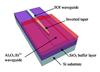 |
| Image of the chip including silicon optical waveguide (SOI: silicon on insulator) as well as erbium-doped aluminium oxyde. |
Abstract:
Within optical microchips, light finds its way through channels, waveguides, made of silicon. Light from a glass fiber, for example, is led through a structure of optical channels with splitters and couplers. Silicon is the workhorse for this, but it is still passive conduction of light, with some losses as well. To be able to amplify the signal, or even to include a light source on the chip, extra steps are necessary. Other types of semiconductors, like Gallium Arsenide, are an option. But materials doped with the rare earth material erbium have good amplification properties as well.
Ultra fast optical amplifier: silicon and erbium on one chip for the first time
Enschede, Netherlands | Posted on September 22nd, 2012Until now, no chip existed, on which both silicon and erbium-doped material were integrated. In her thesis, PhD candidate Laura Agazzi of the University of Twente demonstrates a working chip for the first time. It will be able to amplify light at speeds up to 170 Gbit/sec. The prototype chip has a signal gain of 7.2 decibel at infrared light (1533 nanometer).
The prototype is a starting point, but the results are very promising. One of the possibilities is a laser with an extremely narrow linewidth of 1.7 kHz. "In any application that needs emission or amplification of light, this integration of both materials is useful. It is not limited to telecom. You could use these chips for sensor purposes, for tracing extremely small particles, for example," Agazzi adds.
Trade-off
Laura Agazzi has investigated the optical properties of aluminium oxide doped with erbium, to understand the mechanisms that influence the amplification properties in a negative way. One of these is called energy-transfer up conversion (ETU), which is detrimental for good functionality."If you want a large amplification, you would like to put many erbium ions in the material, this in turn can cause a higher ETU. There are possibilities in adapting the host material, causing less interaction of the ions. With my models, I have gained better insight in these and other mechanisms that lower the amplification.
Laura Agazzi (1983, Vimercate, Italie) conducted her research within the Integrated Optical Microsystems (IOMS) of prof Markus Pollnau, which is part of the MESA+ Institute for Nanotechnology of the University of Twente. On Sep 20 she successfully defended her thesis Spectroscopic Excitation and Quenching Processes in Rare-Earth-Ion-Doped Al2O3 and their Impact on Amplifier and Laser Performance. Her thesis, or a summary, are available digitally.
####
For more information, please click here
Contacts:
Wiebe van der Veen
+31612185692
Copyright © AlphaGalileo
If you have a comment, please Contact us.Issuers of news releases, not 7th Wave, Inc. or Nanotechnology Now, are solely responsible for the accuracy of the content.
Bookmark:


| Related News Press |
News and information
![]() Simulating magnetization in a Heisenberg quantum spin chain April 5th, 2024
Simulating magnetization in a Heisenberg quantum spin chain April 5th, 2024
![]() NRL charters Navy�s quantum inertial navigation path to reduce drift April 5th, 2024
NRL charters Navy�s quantum inertial navigation path to reduce drift April 5th, 2024
![]() Discovery points path to flash-like memory for storing qubits: Rice find could hasten development of nonvolatile quantum memory April 5th, 2024
Discovery points path to flash-like memory for storing qubits: Rice find could hasten development of nonvolatile quantum memory April 5th, 2024
Chip Technology
![]() Discovery points path to flash-like memory for storing qubits: Rice find could hasten development of nonvolatile quantum memory April 5th, 2024
Discovery points path to flash-like memory for storing qubits: Rice find could hasten development of nonvolatile quantum memory April 5th, 2024
![]() Utilizing palladium for addressing contact issues of buried oxide thin film transistors April 5th, 2024
Utilizing palladium for addressing contact issues of buried oxide thin film transistors April 5th, 2024
![]() HKUST researchers develop new integration technique for efficient coupling of III-V and silicon February 16th, 2024
HKUST researchers develop new integration technique for efficient coupling of III-V and silicon February 16th, 2024
Optical computing/Photonic computing
![]() With VECSELs towards the quantum internet Fraunhofer: IAF achieves record output power with VECSEL for quantum frequency converters April 5th, 2024
With VECSELs towards the quantum internet Fraunhofer: IAF achieves record output power with VECSEL for quantum frequency converters April 5th, 2024
![]() Chemical reactions can scramble quantum information as well as black holes April 5th, 2024
Chemical reactions can scramble quantum information as well as black holes April 5th, 2024
![]() Optically trapped quantum droplets of light can bind together to form macroscopic complexes March 8th, 2024
Optically trapped quantum droplets of light can bind together to form macroscopic complexes March 8th, 2024
![]() HKUST researchers develop new integration technique for efficient coupling of III-V and silicon February 16th, 2024
HKUST researchers develop new integration technique for efficient coupling of III-V and silicon February 16th, 2024
Discoveries
![]() Chemical reactions can scramble quantum information as well as black holes April 5th, 2024
Chemical reactions can scramble quantum information as well as black holes April 5th, 2024
![]() New micromaterial releases nanoparticles that selectively destroy cancer cells April 5th, 2024
New micromaterial releases nanoparticles that selectively destroy cancer cells April 5th, 2024
![]() Utilizing palladium for addressing contact issues of buried oxide thin film transistors April 5th, 2024
Utilizing palladium for addressing contact issues of buried oxide thin film transistors April 5th, 2024
Announcements
![]() NRL charters Navy�s quantum inertial navigation path to reduce drift April 5th, 2024
NRL charters Navy�s quantum inertial navigation path to reduce drift April 5th, 2024
![]() Discovery points path to flash-like memory for storing qubits: Rice find could hasten development of nonvolatile quantum memory April 5th, 2024
Discovery points path to flash-like memory for storing qubits: Rice find could hasten development of nonvolatile quantum memory April 5th, 2024
Photonics/Optics/Lasers
![]() With VECSELs towards the quantum internet Fraunhofer: IAF achieves record output power with VECSEL for quantum frequency converters April 5th, 2024
With VECSELs towards the quantum internet Fraunhofer: IAF achieves record output power with VECSEL for quantum frequency converters April 5th, 2024
![]() Nanoscale CL thermometry with lanthanide-doped heavy-metal oxide in TEM March 8th, 2024
Nanoscale CL thermometry with lanthanide-doped heavy-metal oxide in TEM March 8th, 2024
![]() Optically trapped quantum droplets of light can bind together to form macroscopic complexes March 8th, 2024
Optically trapped quantum droplets of light can bind together to form macroscopic complexes March 8th, 2024
![]() HKUST researchers develop new integration technique for efficient coupling of III-V and silicon February 16th, 2024
HKUST researchers develop new integration technique for efficient coupling of III-V and silicon February 16th, 2024
|
|
||
|
|
||
| The latest news from around the world, FREE | ||
|
|
||
|
|
||
| Premium Products | ||
|
|
||
|
Only the news you want to read!
Learn More |
||
|
|
||
|
Full-service, expert consulting
Learn More |
||
|
|
||