Home > Press > Broadband Plasmonic Response of Semiconductor Disks
 |
Abstract:
ecently, there has been a strong interest in tailoring of the spectral characteristics of localized surface plasmons resonances due to potential applications in sensing, imaging, and photovoltaics. Fano-like resonances can be used to control the optical properties only within an extremely narrow frequency window. In contrast, the concept of transformation optics has been proposed to transfer the broad bandwidth behavior of plasmonic waveguides to nanoantennas using geometric singularities. Although efforts have been made to reduce the geometric requirements for these nanostructures, theoretical designs are still largely beyond current nanofabrication capabilities.
Broadband Plasmonic Response of Semiconductor Disks
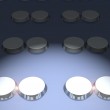
Germany | Posted on September 13th, 2012For the first time Stefan Maier, Steven Hanham (Imperial College London) and co-workers were able to realize such a broadband plasmonic response experimentally by employing a simple strategy. By replacing the usual plasmonic materials with a semiconductor, indium antimonide (InSb), the wavelength of operation shifts from the optical to the terahertz regime. This shift in length scale greatly facilitates the device fabrication. They could show that a touching disk geometry results in a broadband absorption response consistent with the theoretical predictions of transformation optics for gold nanostructures at visible frequencies.
This study proves that semiconductors are extremely useful materials to test plasmonic devices whose fabrication requirements are still out of reach in the optical regime. The presented efficient broadband terahertz harvesting properties of touching InSb disks will definitely find applications in technological areas such as spectroscopy, biosensing, and security.
The research was reported in Advanced Optical Materials, a new section in Advanced Materials dedicated to breakthrough discoveries and fundamental research in photonics, plasmonics, metamaterials, and more, covering all aspects of light-matter interactions.
####
For more information, please click here
Copyright © Wiley-VCH Materials Science Journals
If you have a comment, please Contact us.Issuers of news releases, not 7th Wave, Inc. or Nanotechnology Now, are solely responsible for the accuracy of the content.
Bookmark:


| Related Links |
![]() To get Advanced Optical Materials email alerts, click here:
To get Advanced Optical Materials email alerts, click here:
![]() Link to the original paper on Wiley Online Library
Link to the original paper on Wiley Online Library
| Related News Press |
News and information
![]() Simulating magnetization in a Heisenberg quantum spin chain April 5th, 2024
Simulating magnetization in a Heisenberg quantum spin chain April 5th, 2024
![]() NRL charters Navy�s quantum inertial navigation path to reduce drift April 5th, 2024
NRL charters Navy�s quantum inertial navigation path to reduce drift April 5th, 2024
![]() Discovery points path to flash-like memory for storing qubits: Rice find could hasten development of nonvolatile quantum memory April 5th, 2024
Discovery points path to flash-like memory for storing qubits: Rice find could hasten development of nonvolatile quantum memory April 5th, 2024
Imaging
![]() Nanoscale CL thermometry with lanthanide-doped heavy-metal oxide in TEM March 8th, 2024
Nanoscale CL thermometry with lanthanide-doped heavy-metal oxide in TEM March 8th, 2024
![]() The USTC realizes In situ electron paramagnetic resonance spectroscopy using single nanodiamond sensors November 3rd, 2023
The USTC realizes In situ electron paramagnetic resonance spectroscopy using single nanodiamond sensors November 3rd, 2023
![]() Observation of left and right at nanoscale with optical force October 6th, 2023
Observation of left and right at nanoscale with optical force October 6th, 2023
Sensors
Discoveries
![]() Chemical reactions can scramble quantum information as well as black holes April 5th, 2024
Chemical reactions can scramble quantum information as well as black holes April 5th, 2024
![]() New micromaterial releases nanoparticles that selectively destroy cancer cells April 5th, 2024
New micromaterial releases nanoparticles that selectively destroy cancer cells April 5th, 2024
![]() Utilizing palladium for addressing contact issues of buried oxide thin film transistors April 5th, 2024
Utilizing palladium for addressing contact issues of buried oxide thin film transistors April 5th, 2024
Announcements
![]() NRL charters Navy�s quantum inertial navigation path to reduce drift April 5th, 2024
NRL charters Navy�s quantum inertial navigation path to reduce drift April 5th, 2024
![]() Discovery points path to flash-like memory for storing qubits: Rice find could hasten development of nonvolatile quantum memory April 5th, 2024
Discovery points path to flash-like memory for storing qubits: Rice find could hasten development of nonvolatile quantum memory April 5th, 2024
Energy
![]() Development of zinc oxide nanopagoda array photoelectrode: photoelectrochemical water-splitting hydrogen production January 12th, 2024
Development of zinc oxide nanopagoda array photoelectrode: photoelectrochemical water-splitting hydrogen production January 12th, 2024
![]() Shedding light on unique conduction mechanisms in a new type of perovskite oxide November 17th, 2023
Shedding light on unique conduction mechanisms in a new type of perovskite oxide November 17th, 2023
![]() Inverted perovskite solar cell breaks 25% efficiency record: Researchers improve cell efficiency using a combination of molecules to address different November 17th, 2023
Inverted perovskite solar cell breaks 25% efficiency record: Researchers improve cell efficiency using a combination of molecules to address different November 17th, 2023
![]() The efficient perovskite cells with a structured anti-reflective layer � another step towards commercialization on a wider scale October 6th, 2023
The efficient perovskite cells with a structured anti-reflective layer � another step towards commercialization on a wider scale October 6th, 2023
Photonics/Optics/Lasers
![]() With VECSELs towards the quantum internet Fraunhofer: IAF achieves record output power with VECSEL for quantum frequency converters April 5th, 2024
With VECSELs towards the quantum internet Fraunhofer: IAF achieves record output power with VECSEL for quantum frequency converters April 5th, 2024
![]() Nanoscale CL thermometry with lanthanide-doped heavy-metal oxide in TEM March 8th, 2024
Nanoscale CL thermometry with lanthanide-doped heavy-metal oxide in TEM March 8th, 2024
![]() Optically trapped quantum droplets of light can bind together to form macroscopic complexes March 8th, 2024
Optically trapped quantum droplets of light can bind together to form macroscopic complexes March 8th, 2024
![]() HKUST researchers develop new integration technique for efficient coupling of III-V and silicon February 16th, 2024
HKUST researchers develop new integration technique for efficient coupling of III-V and silicon February 16th, 2024
Solar/Photovoltaic
![]() Development of zinc oxide nanopagoda array photoelectrode: photoelectrochemical water-splitting hydrogen production January 12th, 2024
Development of zinc oxide nanopagoda array photoelectrode: photoelectrochemical water-splitting hydrogen production January 12th, 2024
![]() Shedding light on unique conduction mechanisms in a new type of perovskite oxide November 17th, 2023
Shedding light on unique conduction mechanisms in a new type of perovskite oxide November 17th, 2023
![]() Inverted perovskite solar cell breaks 25% efficiency record: Researchers improve cell efficiency using a combination of molecules to address different November 17th, 2023
Inverted perovskite solar cell breaks 25% efficiency record: Researchers improve cell efficiency using a combination of molecules to address different November 17th, 2023
![]() Charged �molecular beasts� the basis for new compounds: Researchers at Leipzig University use �aggressive� fragments of molecular ions for chemical synthesis November 3rd, 2023
Charged �molecular beasts� the basis for new compounds: Researchers at Leipzig University use �aggressive� fragments of molecular ions for chemical synthesis November 3rd, 2023
|
|
||
|
|
||
| The latest news from around the world, FREE | ||
|
|
||
|
|
||
| Premium Products | ||
|
|
||
|
Only the news you want to read!
Learn More |
||
|
|
||
|
Full-service, expert consulting
Learn More |
||
|
|
||