Home > Press > New technique could mean super thin, strong graphene-based circuits
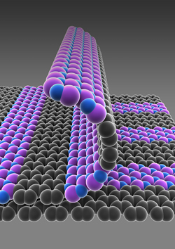 |
| Provided/Jiwoong Park Schematic illustration of single-atom-thick films with patterned regions of conducting graphene (gray) and insulating boron nitride (purple-blue). |
Abstract:
Integrated circuits, which are in everything from coffeemakers to computers and are patterned from perfectly crystalline silicon, are quite thin -- but Cornell researchers think they can push thin-film boundaries to the single-atom level.
New technique could mean super thin, strong graphene-based circuits
Ithaca, NY | Posted on August 29th, 2012Their materials of choice are graphene, single atom-thick sheets of repeating carbon atoms, and hexagonal boron nitride, similarly thin sheets of repeating boron and nitrogen atoms. Researchers led by Jiwoong Park, assistant professor of chemistry and chemical biology, have invented a way to pattern single atom films of graphene and boron nitride, an insulator, without the use of a silicon substrate. The work is detailed in an article in the journal Nature, published online Aug. 30.
The technique, which they call patterned regrowth, could lead to substrate-free, atomically thin circuits -- so thin, they could float on water or through air, but with tensile strength and top-notch electrical performance.
"We know how to grow graphene in single atom-thick films, and we know how to grow boron nitride," Park said. "But can we bring them together side and side? And when you bring them together, what happens at their junctions?"
As it turns out, researchers' patterned regrowth, which harnesses the same basic photolithography technology used in silicon wafer processing, allows graphene and boron nitride to grow in perfectly flat, structurally smooth films -- no creases or bumps, like a well-knitted scarf -- which, if combined with the final, yet to be realized step of introducing a semiconductor material, could lead to the first atomically thin integrated circuit.
Simple really is beautiful, especially in the case of thin films, because photolithography is a well-established technique that forms the basis for making integrated circuits by laying materials, one layer at a time, on flat silicon.
Patterned regrowth is a bit like stenciling, Park said. He and colleagues first grew graphene on copper and used photolithography to expose graphene on selected areas, depending on the desired pattern. They filled that exposed copper surface with boron nitride, the insulator, which grows on copper and "fills the gaps in very nicely."
"In the end, it forms a very nice cloth you just peel off," Park said.
The research team, which includes David A. Muller, professor of applied and engineering physics, is working to determine what material would best work with graphene-boron nitride thin films to make up the final semiconducting layer that could turn the films into actual devices.
The team was helped by already being skilled at making graphene -- still relatively new in the materials world -- as well as Muller's expertise in electron microscopy characterization at the nanoscale. Muller helped the team confirm that the lateral junctions of the two materials were, indeed, smooth and well connected.
The paper's co-first authors were chemistry graduate student Mark Levendorf and postdoctoral associate Cheol-Joo Kim, who fabricated the graphene and boron nitride samples and also performed the patterned regrowth at the Cornell NanoScale Science and Technology Facility.
The work was supported primarily by the Air Force Office of Scientific Research, and the National Science Foundation through the Cornell Center for Materials Research.
####
For more information, please click here
Contacts:
Media Contact:
Syl Kacapyr
(607) 255-7701
Cornell Chronicle:
Anne Ju
(607) 255-9735
Copyright © Cornell University
If you have a comment, please Contact us.Issuers of news releases, not 7th Wave, Inc. or Nanotechnology Now, are solely responsible for the accuracy of the content.
Bookmark:


| Related News Press |
News and information
![]() Simulating magnetization in a Heisenberg quantum spin chain April 5th, 2024
Simulating magnetization in a Heisenberg quantum spin chain April 5th, 2024
![]() NRL charters Navy�s quantum inertial navigation path to reduce drift April 5th, 2024
NRL charters Navy�s quantum inertial navigation path to reduce drift April 5th, 2024
![]() Discovery points path to flash-like memory for storing qubits: Rice find could hasten development of nonvolatile quantum memory April 5th, 2024
Discovery points path to flash-like memory for storing qubits: Rice find could hasten development of nonvolatile quantum memory April 5th, 2024
![]() Good as gold - improving infectious disease testing with gold nanoparticles April 5th, 2024
Good as gold - improving infectious disease testing with gold nanoparticles April 5th, 2024
Thin films
![]() Utilizing palladium for addressing contact issues of buried oxide thin film transistors April 5th, 2024
Utilizing palladium for addressing contact issues of buried oxide thin film transistors April 5th, 2024
Graphene/ Graphite
![]() NRL discovers two-dimensional waveguides February 16th, 2024
NRL discovers two-dimensional waveguides February 16th, 2024
Govt.-Legislation/Regulation/Funding/Policy
![]() NRL charters Navy�s quantum inertial navigation path to reduce drift April 5th, 2024
NRL charters Navy�s quantum inertial navigation path to reduce drift April 5th, 2024
![]() Discovery points path to flash-like memory for storing qubits: Rice find could hasten development of nonvolatile quantum memory April 5th, 2024
Discovery points path to flash-like memory for storing qubits: Rice find could hasten development of nonvolatile quantum memory April 5th, 2024
![]() Chemical reactions can scramble quantum information as well as black holes April 5th, 2024
Chemical reactions can scramble quantum information as well as black holes April 5th, 2024
Discoveries
![]() Chemical reactions can scramble quantum information as well as black holes April 5th, 2024
Chemical reactions can scramble quantum information as well as black holes April 5th, 2024
![]() New micromaterial releases nanoparticles that selectively destroy cancer cells April 5th, 2024
New micromaterial releases nanoparticles that selectively destroy cancer cells April 5th, 2024
![]() Utilizing palladium for addressing contact issues of buried oxide thin film transistors April 5th, 2024
Utilizing palladium for addressing contact issues of buried oxide thin film transistors April 5th, 2024
Announcements
![]() NRL charters Navy�s quantum inertial navigation path to reduce drift April 5th, 2024
NRL charters Navy�s quantum inertial navigation path to reduce drift April 5th, 2024
![]() Discovery points path to flash-like memory for storing qubits: Rice find could hasten development of nonvolatile quantum memory April 5th, 2024
Discovery points path to flash-like memory for storing qubits: Rice find could hasten development of nonvolatile quantum memory April 5th, 2024
Military
![]() NRL charters Navy�s quantum inertial navigation path to reduce drift April 5th, 2024
NRL charters Navy�s quantum inertial navigation path to reduce drift April 5th, 2024
![]() What heat can tell us about battery chemistry: using the Peltier effect to study lithium-ion cells March 8th, 2024
What heat can tell us about battery chemistry: using the Peltier effect to study lithium-ion cells March 8th, 2024
![]() New chip opens door to AI computing at light speed February 16th, 2024
New chip opens door to AI computing at light speed February 16th, 2024
|
|
||
|
|
||
| The latest news from around the world, FREE | ||
|
|
||
|
|
||
| Premium Products | ||
|
|
||
|
Only the news you want to read!
Learn More |
||
|
|
||
|
Full-service, expert consulting
Learn More |
||
|
|
||