Home > Press > Flat lens offers a perfect image: Ultrathin wafer of silicon and gold focuses telecom wavelengths without distortion
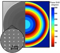 |
| Left: A micrograph of the flat lens (diameter approximately 1 mm) made of silicon. The surface is coated with concentric rings of gold optical nanoantennas (inset) which impart different delays to the light traversing the lens. Right:The colored rings show the magnitude of the phase delay corresponding to each ring. (Image courtesy of Francesco Aieta.) |
Abstract:
Applied physicists at the Harvard School of Engineering and Applied Sciences (SEAS) have created an ultrathin, flat lens that focuses light without imparting the distortions of conventional lenses.
Flat lens offers a perfect image: Ultrathin wafer of silicon and gold focuses telecom wavelengths without distortion
Cambridge, MA | Posted on August 24th, 2012At a mere 60 nanometers thick, the flat lens is essentially two-dimensional, yet its focusing power approaches the ultimate physical limit set by the laws of diffraction.
Operating at telecom wavelengths (i.e., the range commonly used in fiber-optic communications), the new device is completely scalable, from near-infrared to terahertz wavelengths, and simple to manufacture. The results have been published online in the journal Nano Letters.
"Our flat lens opens up a new type of technology," says principal investigator Federico Capasso, Robert L. Wallace Professor of Applied Physics and Vinton Hayes Senior Research Fellow in Electrical Engineering at SEAS. "We're presenting a new way of making lenses. Instead of creating phase delays as light propagates through the thickness of the material, you can create an instantaneous phase shift right at the surface of the lens. It's extremely exciting."
Capasso and his collaborators at SEAS create the flat lens by plating a very thin wafer of silicon with an nanometer-thin layer of gold. Next, they strip away parts of the gold layer to leave behind an array of V-shaped structures, evenly spaced in rows across the surface. When Capasso's group shines a laser onto the flat lens, these structures act as nanoantennas that capture the incoming light and hold onto it briefly before releasing it again. Those delays, which are precisely tuned across the surface of the lens, change the direction of the light in the same way that a thick glass lens would, with an important distinction.
The flat lens eliminates optical aberrations such as the "fish-eye" effect that results from conventional wide-angle lenses. Astigmatism and coma aberrations also do not occur with the flat lens, so the resulting image or signal is completely accurate and does not require any complex corrective techniques.
The array of nanoantennas, dubbed a "metasurface," can be tuned for specific wavelengths of light by simply changing the size, angle, and spacing of the antennas.
"In the future we can potentially replace all the bulk components in the majority of optical systems with just flat surfaces," says lead author Francesco Aieta, a visiting graduate student from the Universit� Politecnica delle Marche in Italy. "It certainly captures the imagination."
####
About Harvard's School of Engineering and Applied Sciences (SEAS)
Aieta�s and Capasso�s coauthors at SEAS included postdoctoral research associates Patrice Genevet and Nanfang Yu (Ph.D. �09), graduate students Mikhail A. Kats and Romain Blanchard, and visiting scholar Zeno Gaburro.
The work was supported by the National Science Foundation (NSF), the NSF-funded Harvard Nanoscale Science and Engineering Center, and the Center for Nanoscale Systems at Harvard (a member of the NSF-supported National Nanotechnology Infrastructure Network). The researchers also individually received support from the Robert A. Welch Foundation, the European Communities Seventh Framework Programme, and an NSF Graduate Research Fellowship.
For more information, please click here
Contacts:
Caroline Perry
(617) 496-1351
Copyright © Harvard's School of Engineering and Applied Sciences (SEAS)
If you have a comment, please Contact us.Issuers of news releases, not 7th Wave, Inc. or Nanotechnology Now, are solely responsible for the accuracy of the content.
Bookmark:


| Related News Press |
News and information
![]() Simulating magnetization in a Heisenberg quantum spin chain April 5th, 2024
Simulating magnetization in a Heisenberg quantum spin chain April 5th, 2024
![]() NRL charters Navy�s quantum inertial navigation path to reduce drift April 5th, 2024
NRL charters Navy�s quantum inertial navigation path to reduce drift April 5th, 2024
![]() Discovery points path to flash-like memory for storing qubits: Rice find could hasten development of nonvolatile quantum memory April 5th, 2024
Discovery points path to flash-like memory for storing qubits: Rice find could hasten development of nonvolatile quantum memory April 5th, 2024
Govt.-Legislation/Regulation/Funding/Policy
![]() NRL charters Navy�s quantum inertial navigation path to reduce drift April 5th, 2024
NRL charters Navy�s quantum inertial navigation path to reduce drift April 5th, 2024
![]() Discovery points path to flash-like memory for storing qubits: Rice find could hasten development of nonvolatile quantum memory April 5th, 2024
Discovery points path to flash-like memory for storing qubits: Rice find could hasten development of nonvolatile quantum memory April 5th, 2024
![]() Chemical reactions can scramble quantum information as well as black holes April 5th, 2024
Chemical reactions can scramble quantum information as well as black holes April 5th, 2024
Discoveries
![]() Chemical reactions can scramble quantum information as well as black holes April 5th, 2024
Chemical reactions can scramble quantum information as well as black holes April 5th, 2024
![]() New micromaterial releases nanoparticles that selectively destroy cancer cells April 5th, 2024
New micromaterial releases nanoparticles that selectively destroy cancer cells April 5th, 2024
![]() Utilizing palladium for addressing contact issues of buried oxide thin film transistors April 5th, 2024
Utilizing palladium for addressing contact issues of buried oxide thin film transistors April 5th, 2024
Announcements
![]() NRL charters Navy�s quantum inertial navigation path to reduce drift April 5th, 2024
NRL charters Navy�s quantum inertial navigation path to reduce drift April 5th, 2024
![]() Discovery points path to flash-like memory for storing qubits: Rice find could hasten development of nonvolatile quantum memory April 5th, 2024
Discovery points path to flash-like memory for storing qubits: Rice find could hasten development of nonvolatile quantum memory April 5th, 2024
Grants/Sponsored Research/Awards/Scholarships/Gifts/Contests/Honors/Records
![]() Discovery points path to flash-like memory for storing qubits: Rice find could hasten development of nonvolatile quantum memory April 5th, 2024
Discovery points path to flash-like memory for storing qubits: Rice find could hasten development of nonvolatile quantum memory April 5th, 2024
![]() Chemical reactions can scramble quantum information as well as black holes April 5th, 2024
Chemical reactions can scramble quantum information as well as black holes April 5th, 2024
Photonics/Optics/Lasers
![]() With VECSELs towards the quantum internet Fraunhofer: IAF achieves record output power with VECSEL for quantum frequency converters April 5th, 2024
With VECSELs towards the quantum internet Fraunhofer: IAF achieves record output power with VECSEL for quantum frequency converters April 5th, 2024
![]() Nanoscale CL thermometry with lanthanide-doped heavy-metal oxide in TEM March 8th, 2024
Nanoscale CL thermometry with lanthanide-doped heavy-metal oxide in TEM March 8th, 2024
![]() Optically trapped quantum droplets of light can bind together to form macroscopic complexes March 8th, 2024
Optically trapped quantum droplets of light can bind together to form macroscopic complexes March 8th, 2024
![]() HKUST researchers develop new integration technique for efficient coupling of III-V and silicon February 16th, 2024
HKUST researchers develop new integration technique for efficient coupling of III-V and silicon February 16th, 2024
|
|
||
|
|
||
| The latest news from around the world, FREE | ||
|
|
||
|
|
||
| Premium Products | ||
|
|
||
|
Only the news you want to read!
Learn More |
||
|
|
||
|
Full-service, expert consulting
Learn More |
||
|
|
||