Home > Press > Patterning defect-free nanocrystal films with nanometer resolution: New process developed at MIT could enable better LED displays, solar cells and biosensors — and foster basic physics research
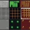 |
| Images of nanopatterned films of nano crystalline material produced by the MIT research team. Each row shows a different pattern produced on films of either cadmium selenide (top and bottom) or a combination of zinc cadmium selenide and zinc cadmium sulfur (middle row). The three images in each row are made using different kinds of microscopes: left to right, scanning electron microscope, optical (showing real-color fluorescence), and atomic force microscope. Images courtesy of Mentzel et al, from Nano Letters |
Abstract:
Films made of semiconductor nanocrystals — tiny crystals measuring just a few billionths of a meter across — are seen as a promising new material for a wide range of applications. Nanocrystals could be used in electronic or photonic circuits, detectors for biomolecules, or the glowing pixels on high-resolution display screens. They also hold promise for more efficient solar cells.
Patterning defect-free nanocrystal films with nanometer resolution: New process developed at MIT could enable better LED displays, solar cells and biosensors — and foster basic physics research
Cambridge, MA | Posted on August 20th, 2012The size of a semiconductor nanocrystal determines its electrical and optical properties. But it's very hard to control the placement of nanocrystals on a surface in order to make structurally uniform films. Typical nanocrystal films also have cracks that limit their usefulness and make it impossible to measure the fundamental properties of these materials.
Now, researchers at MIT say they have found ways of making defect-free patterns of nanocrystal films where the shape and position of the films are controlled with nanoscale resolution, potentially opening up a significant area for research and possible new applications.
"We've been trying to understand how electrons move in arrays of these nanocrystals," which has been difficult with limited control over the formation of the arrays, says physicist Marc Kastner, the Donner Professor of Science, dean of MIT's School of Science and senior author of a paper published online in the journal Nano Letters.
The work builds on research by Moungi Bawendi, the Lester Wolfe Professor of Chemistry at MIT and a co-author of this paper, who was one of the first researchers to precisely control nanocrystal production. Such control made it possible, among other things, to produce materials that glow, or fluoresce, in a range of different colors based on their sizes — even though they are all made of the same material.
In the initial phases of the new work, postdoc Tamar Mentzel produced nanoscale patterns that emit invisible infrared light. But working on such systems is tedious, since each fine-tuning has to be checked using time-consuming electron microscopy. So when Mentzel succeeded in getting semiconductor nanocrystal patterns to glow with visible light, making them visible through an optical microscope, it meant that the team could greatly speed the development of the new technology. "Even though the nanoscale patterns are below the resolution limit of the optical microscope, the nanocrystals act as a light source, rendering them visible," Mentzel says.
The electrical conductivity of the researchers' defect-free films is roughly 180 times greater than that of the cracked films made by conventional methods. In addition, the process developed by the MIT team has already made it possible to create patterns on a silicon surface that are just 30 nanometers across — about the size of the finest features possible with present manufacturing techniques.
The process is unique in producing such tiny patterns of defect-free films, Mentzel says. "The trick was to get the film to be uniform, and to stick" to the silicon dioxide substrate, Kastner adds. That was achieved by leaving a thin layer of polymer to coat the surface before depositing the layer of nanocrystals on top of it. The researchers conjecture that tiny organic molecules on the surface of the nanocrystals help them bind to the polymer layer.
Such nanocrystal patterns could have many applications, Kastner says. Because these nanocrystals can be tuned not only to emit but also to absorb a wide spectrum of colors of light, they could enable a new kind of broad-spectrum solar cell, he says.
But Kastner and Mentzel's personal interest has more to do with basic physics: Since the minuscule crystals behave almost like oversized atoms, the researchers aim to use the arrays to study fundamental processes of solids, Mentzel says. The success of this technique has already enabled new research on how electrons move in the films.
Such materials could also be used to develop sensitive detectors for tiny amounts of certain biological molecules, either as screening systems for toxins or as medical testing devices, the researchers say.
Douglas Natelson, a professor of physics and astronomy at Rice University who was not involved in this work, says, "The challenge in the past has been achieving thin, uniform films, patterned at high resolution, with good contact between the nanocrystals and no cracking." The MIT team's approach, he says, "while deceptively simple in appearance, accomplishes all of these objectives."
Natelson adds: "I think this is a very nice achievement. The fluorescence images showing the nanopatterned films are eye-popping, particularly for those who know how tough this is."
The research was supported by the U.S Army Research Office, the Department of Energy and Samsung.
Written by: David L. Chandler, MIT News Office
####
For more information, please click here
Contacts:
Caroline McCall
MIT News Office
617-253-1682
Copyright © MIT
If you have a comment, please Contact us.Issuers of news releases, not 7th Wave, Inc. or Nanotechnology Now, are solely responsible for the accuracy of the content.
Bookmark:


| Related News Press |
News and information
![]() Simulating magnetization in a Heisenberg quantum spin chain April 5th, 2024
Simulating magnetization in a Heisenberg quantum spin chain April 5th, 2024
![]() NRL charters Navy’s quantum inertial navigation path to reduce drift April 5th, 2024
NRL charters Navy’s quantum inertial navigation path to reduce drift April 5th, 2024
![]() Discovery points path to flash-like memory for storing qubits: Rice find could hasten development of nonvolatile quantum memory April 5th, 2024
Discovery points path to flash-like memory for storing qubits: Rice find could hasten development of nonvolatile quantum memory April 5th, 2024
![]() Good as gold - improving infectious disease testing with gold nanoparticles April 5th, 2024
Good as gold - improving infectious disease testing with gold nanoparticles April 5th, 2024
Thin films
![]() Utilizing palladium for addressing contact issues of buried oxide thin film transistors April 5th, 2024
Utilizing palladium for addressing contact issues of buried oxide thin film transistors April 5th, 2024
Display technology/LEDs/SS Lighting/OLEDs
![]() Utilizing palladium for addressing contact issues of buried oxide thin film transistors April 5th, 2024
Utilizing palladium for addressing contact issues of buried oxide thin film transistors April 5th, 2024
![]() Light guide plate based on perovskite nanocomposites November 3rd, 2023
Light guide plate based on perovskite nanocomposites November 3rd, 2023
![]() Simple ballpoint pen can write custom LEDs August 11th, 2023
Simple ballpoint pen can write custom LEDs August 11th, 2023
Govt.-Legislation/Regulation/Funding/Policy
![]() NRL charters Navy’s quantum inertial navigation path to reduce drift April 5th, 2024
NRL charters Navy’s quantum inertial navigation path to reduce drift April 5th, 2024
![]() Discovery points path to flash-like memory for storing qubits: Rice find could hasten development of nonvolatile quantum memory April 5th, 2024
Discovery points path to flash-like memory for storing qubits: Rice find could hasten development of nonvolatile quantum memory April 5th, 2024
![]() Chemical reactions can scramble quantum information as well as black holes April 5th, 2024
Chemical reactions can scramble quantum information as well as black holes April 5th, 2024
Chip Technology
![]() Discovery points path to flash-like memory for storing qubits: Rice find could hasten development of nonvolatile quantum memory April 5th, 2024
Discovery points path to flash-like memory for storing qubits: Rice find could hasten development of nonvolatile quantum memory April 5th, 2024
![]() Utilizing palladium for addressing contact issues of buried oxide thin film transistors April 5th, 2024
Utilizing palladium for addressing contact issues of buried oxide thin film transistors April 5th, 2024
![]() HKUST researchers develop new integration technique for efficient coupling of III-V and silicon February 16th, 2024
HKUST researchers develop new integration technique for efficient coupling of III-V and silicon February 16th, 2024
Sensors
Discoveries
![]() Chemical reactions can scramble quantum information as well as black holes April 5th, 2024
Chemical reactions can scramble quantum information as well as black holes April 5th, 2024
![]() New micromaterial releases nanoparticles that selectively destroy cancer cells April 5th, 2024
New micromaterial releases nanoparticles that selectively destroy cancer cells April 5th, 2024
![]() Utilizing palladium for addressing contact issues of buried oxide thin film transistors April 5th, 2024
Utilizing palladium for addressing contact issues of buried oxide thin film transistors April 5th, 2024
Announcements
![]() NRL charters Navy’s quantum inertial navigation path to reduce drift April 5th, 2024
NRL charters Navy’s quantum inertial navigation path to reduce drift April 5th, 2024
![]() Discovery points path to flash-like memory for storing qubits: Rice find could hasten development of nonvolatile quantum memory April 5th, 2024
Discovery points path to flash-like memory for storing qubits: Rice find could hasten development of nonvolatile quantum memory April 5th, 2024
Military
![]() NRL charters Navy’s quantum inertial navigation path to reduce drift April 5th, 2024
NRL charters Navy’s quantum inertial navigation path to reduce drift April 5th, 2024
![]() What heat can tell us about battery chemistry: using the Peltier effect to study lithium-ion cells March 8th, 2024
What heat can tell us about battery chemistry: using the Peltier effect to study lithium-ion cells March 8th, 2024
![]() New chip opens door to AI computing at light speed February 16th, 2024
New chip opens door to AI computing at light speed February 16th, 2024
Energy
![]() Development of zinc oxide nanopagoda array photoelectrode: photoelectrochemical water-splitting hydrogen production January 12th, 2024
Development of zinc oxide nanopagoda array photoelectrode: photoelectrochemical water-splitting hydrogen production January 12th, 2024
![]() Shedding light on unique conduction mechanisms in a new type of perovskite oxide November 17th, 2023
Shedding light on unique conduction mechanisms in a new type of perovskite oxide November 17th, 2023
![]() Inverted perovskite solar cell breaks 25% efficiency record: Researchers improve cell efficiency using a combination of molecules to address different November 17th, 2023
Inverted perovskite solar cell breaks 25% efficiency record: Researchers improve cell efficiency using a combination of molecules to address different November 17th, 2023
![]() The efficient perovskite cells with a structured anti-reflective layer – another step towards commercialization on a wider scale October 6th, 2023
The efficient perovskite cells with a structured anti-reflective layer – another step towards commercialization on a wider scale October 6th, 2023
Photonics/Optics/Lasers
![]() With VECSELs towards the quantum internet Fraunhofer: IAF achieves record output power with VECSEL for quantum frequency converters April 5th, 2024
With VECSELs towards the quantum internet Fraunhofer: IAF achieves record output power with VECSEL for quantum frequency converters April 5th, 2024
![]() Nanoscale CL thermometry with lanthanide-doped heavy-metal oxide in TEM March 8th, 2024
Nanoscale CL thermometry with lanthanide-doped heavy-metal oxide in TEM March 8th, 2024
![]() Optically trapped quantum droplets of light can bind together to form macroscopic complexes March 8th, 2024
Optically trapped quantum droplets of light can bind together to form macroscopic complexes March 8th, 2024
![]() HKUST researchers develop new integration technique for efficient coupling of III-V and silicon February 16th, 2024
HKUST researchers develop new integration technique for efficient coupling of III-V and silicon February 16th, 2024
Solar/Photovoltaic
![]() Development of zinc oxide nanopagoda array photoelectrode: photoelectrochemical water-splitting hydrogen production January 12th, 2024
Development of zinc oxide nanopagoda array photoelectrode: photoelectrochemical water-splitting hydrogen production January 12th, 2024
![]() Shedding light on unique conduction mechanisms in a new type of perovskite oxide November 17th, 2023
Shedding light on unique conduction mechanisms in a new type of perovskite oxide November 17th, 2023
![]() Inverted perovskite solar cell breaks 25% efficiency record: Researchers improve cell efficiency using a combination of molecules to address different November 17th, 2023
Inverted perovskite solar cell breaks 25% efficiency record: Researchers improve cell efficiency using a combination of molecules to address different November 17th, 2023
![]() Charged “molecular beasts” the basis for new compounds: Researchers at Leipzig University use “aggressive” fragments of molecular ions for chemical synthesis November 3rd, 2023
Charged “molecular beasts” the basis for new compounds: Researchers at Leipzig University use “aggressive” fragments of molecular ions for chemical synthesis November 3rd, 2023
|
|
||
|
|
||
| The latest news from around the world, FREE | ||
|
|
||
|
|
||
| Premium Products | ||
|
|
||
|
Only the news you want to read!
Learn More |
||
|
|
||
|
Full-service, expert consulting
Learn More |
||
|
|
||