Home > Press > The power to heal at the tips of your fingers
 |
Abstract:
The intricate properties of the fingertips have been mimicked and recreated using semiconductor devices in what researchers hope will lead to the development of advanced surgical gloves.
The power to heal at the tips of your fingers
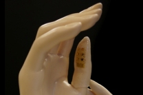
London, UK | Posted on August 11th, 2012The devices, shown to be capable of responding with high precision to the stresses and strains associated with touch and finger movement, are a step towards the creation of surgical gloves for use in medical procedures such as local ablations and ultrasound scans.
Researchers from the University of Illinois at Urbana-Champaign, Northwestern University and Dalian University of Technology have published their study today, Friday 10 August, in IOP Publishing's journal Nanotechnology.
Offering guidelines to the creation of these electrotactile stimulation devices for use on surgeons' fingertips, their paper describes the materials, fabrication strategies and device designs, using ultrathin, stretchable, silicon-based electronics and soft sensors that can be mounted onto an artificial �skin' and fitted to fingertips.
"Imagine the ability to sense the electrical properties of tissue, and then locally remove that tissue, precisely by local ablation, all via the fingertips using smart surgical gloves. Alternatively, or perhaps in addition, ultrasound imaging could be possible," said co-author of the study Professor John Rogers.
The researchers suggest that the new technology could open up possibilities for surgical robots that can interact, in a soft contacting mode, with their surroundings through touch.
The electronic circuit on the �skin' is made of patterns of gold conductive lines and ultrathin sheets of silicon, integrated onto a flexible polymer called polyimide. The sheet is then etched into an open mesh geometry and transferred to a thin sheet of silicone rubber moulded into the precise shape of a finger.
This electronic �skin', or finger cuff, was designed to measure the stresses and strains at the fingertip by measuring the change in capacitance - the ability to store electrical charge - of pairs of microelectrodes in the circuit. Applied forces decreased the spacing in the skin which, in turn, increased the capacitance.
The fingertip device could also be fitted with sensors for measuring motion and temperature, with small-scale heaters as actuators for ablation and other related operations
The researchers experimented with having the electronics on the inside of the device, in contact with wearer's skin, and also on the outside. They believe that because the device exploits materials and fabrication techniques adopted from the established semiconductor industry, the processes can be scaled for realistic use at reasonable cost.
"Perhaps the most important result is that we are able to incorporate multifunctional, silicon semiconductor device technologies into the form of soft, three-dimensional, form-fitting skins, suitable for integration not only with the fingertips but also other parts of the body," continued Professor Rogers.
Indeed, the researchers now intend to create a �skin' for integration on other parts of the body, such as the heart. In this case, a device would envelop the entire 3D surface of the heart, like a sock, to provide various sensing and actuating functions, providing advanced surgical and diagnostic devices relevant to cardiac arrhythmias.
Future challenges include creating materials and schemes to provide the device with wireless data and power.
####
For more information, please click here
Contacts:
Institute of Physics
76 Portland Place
London W1B 1NT
UK
Tel: +44 (0)20 7470 4800
Fax: +44 (0)20 7470 4848
Copyright © Institute of Physics (IOP)
If you have a comment, please Contact us.Issuers of news releases, not 7th Wave, Inc. or Nanotechnology Now, are solely responsible for the accuracy of the content.
Bookmark:


| Related News Press |
News and information
![]() Simulating magnetization in a Heisenberg quantum spin chain April 5th, 2024
Simulating magnetization in a Heisenberg quantum spin chain April 5th, 2024
![]() NRL charters Navy�s quantum inertial navigation path to reduce drift April 5th, 2024
NRL charters Navy�s quantum inertial navigation path to reduce drift April 5th, 2024
![]() Discovery points path to flash-like memory for storing qubits: Rice find could hasten development of nonvolatile quantum memory April 5th, 2024
Discovery points path to flash-like memory for storing qubits: Rice find could hasten development of nonvolatile quantum memory April 5th, 2024
Nanomedicine
![]() New micromaterial releases nanoparticles that selectively destroy cancer cells April 5th, 2024
New micromaterial releases nanoparticles that selectively destroy cancer cells April 5th, 2024
![]() Good as gold - improving infectious disease testing with gold nanoparticles April 5th, 2024
Good as gold - improving infectious disease testing with gold nanoparticles April 5th, 2024
![]() Researchers develop artificial building blocks of life March 8th, 2024
Researchers develop artificial building blocks of life March 8th, 2024
Discoveries
![]() Chemical reactions can scramble quantum information as well as black holes April 5th, 2024
Chemical reactions can scramble quantum information as well as black holes April 5th, 2024
![]() New micromaterial releases nanoparticles that selectively destroy cancer cells April 5th, 2024
New micromaterial releases nanoparticles that selectively destroy cancer cells April 5th, 2024
![]() Utilizing palladium for addressing contact issues of buried oxide thin film transistors April 5th, 2024
Utilizing palladium for addressing contact issues of buried oxide thin film transistors April 5th, 2024
Announcements
![]() NRL charters Navy�s quantum inertial navigation path to reduce drift April 5th, 2024
NRL charters Navy�s quantum inertial navigation path to reduce drift April 5th, 2024
![]() Discovery points path to flash-like memory for storing qubits: Rice find could hasten development of nonvolatile quantum memory April 5th, 2024
Discovery points path to flash-like memory for storing qubits: Rice find could hasten development of nonvolatile quantum memory April 5th, 2024
|
|
||
|
|
||
| The latest news from around the world, FREE | ||
|
|
||
|
|
||
| Premium Products | ||
|
|
||
|
Only the news you want to read!
Learn More |
||
|
|
||
|
Full-service, expert consulting
Learn More |
||
|
|
||