Home > Press > Navy Scientists Demonstrate Breakthrough in Tunnel Barrier Technology
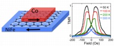 |
| Diagram (left) of the graphene-based magnetic tunnel junction, where a single atom thick layer of carbon atoms in a honeycomb lattice separates two magnetic metal films (cobalt and permalloy). The magnetizations of the films can be aligned parallel or antiparallel, resulting in a change in resistance for current flowing through the structure, called the tunnel magnetoresistance (TMR). The plot (right) shows the TMR as an applied magnetic field changes the relative orientation of the magnetizations — the TMR persists well above room temperature. (U.S. Naval Research Laboratory) |
Abstract:
Scientists at the Naval Research Laboratory have demonstrated, for the first time, the use of graphene as a tunnel barrier — an electrically insulating barrier between two conducting materials through which electrons tunnel quantum mechanically. They report fabrication of magnetic tunnel junctions using graphene, a single atom thick sheet of carbon atoms arranged in a honeycomb lattice, between two ferromagnetic metal layers in a fully scalable photolithographic process. Their results demonstrate that single-layer graphene can function as an effective tunnel barrier for both charge and spin-based devices, and enable realization of more complex graphene-based devices for highly functional nanoscale circuits, such as tunnel transistors, non-volatile magnetic memory and reprogrammable spin logic. These research results are published in the online issue of Nano Letters (14 May 2012; DOI: 10.1021/nl3007616).
Navy Scientists Demonstrate Breakthrough in Tunnel Barrier Technology
Washington, DC | Posted on July 31st, 2012The research initiates a "paradigm shift in tunnel barrier technology for magnetic tunnel junctions (MTJs) used for advanced sensors, memory and logic," explains NRL's Dr. Berend Jonker. Graphene has been the focus of intense research activity because of its remarkable electronic and mechanical properties. In the past, researchers focused on developing graphene as a conductor, or perhaps a semiconductor, where the current flows in-plane parallel to the carbon honeycomb sheet. In contrast, the NRL researchers show that graphene serves as an excellent tunnel barrier when current is directed perpendicular to the plane, and in fact, also preserves the spin polarization of the tunneling current.
Tunnel barriers are the basis for many electronic (charge-based) and spintronic (spin-based) device structures. Fabrication of ultra-thin and defect-free barriers is an ongoing challenge in materials science. Typical tunnel barriers are based on metal oxides (e.g. aluminum oxide or magnesium oxide), and issues such as non-uniform thicknesses, pinholes, defects and trapped charge compromise their performance and reliability. Such oxide tunnel barriers have several limitations which hinder future performance. For example, they have high resistance-area (RA) products which results in higher power consumption and local heating; they allow interdiffusion at the interfaces, which reduces their performance and can lead to catastrophic failure; and their thickness is generally non-uniform, resulting in "hot spots" in the current transport. In contrast, Dr. Jonker explains, the inherent material properties of graphene make it an ideal tunnel barrier. Graphene is chemically inert and impervious to diffusion even at high temperatures. The atomic thickness of graphene represents the ultimate in tunnel barrier scaling for the lowest possible RA product, lowest power consumption and fastest switching speed.
This discovery by NRL researchers is significant because MTJs are widely utilized as read heads in the hard disk drive found in every computer, and as memory elements in non-volatile magnetic random access memory (MRAM) which is rapidly emerging as a universal memory replacement for the many varieties of conventional semiconductor-based memory. They are also considered to be lead contenders as reprogrammable, non-volatile elements for a universal logic block.
Although there has been significant progress, the emerging generation of MTJ-based MRAM relies upon spin-transfer torque switching, and is severely limited by the unacceptably high current densities required to switch the logic state of the cell. The accompanying issues of power consumption and thermal dissipation prevent scaling to higher densities and operation at typical CMOS voltages. The 2011 International Technology Roadmap for Semiconductors (ITRS) states that "all of the existing forms of nonvolatile memory face limitations based on material properties. Success will hinge on finding and developing alternative materials and/or developing alternative emerging technologies ... development of electrically accessible non-volatile memory with high speed and high density would initiate a revolution in computer architecture ... and provide a significant increase in information throughput beyond the traditional benefits of scaling when fully realized for nanoscale CMOS devices" (ITRS 2011 Executive Summary, p28; and Emerging Research Devices, p. 4).
NRL researchers believe that the graphene-based magnetic tunnel junctions they have demonstrated will eclipse the performance and ease of fabrication of existing oxide technology. These graphene-based MTJs would be a breakthrough for nascent spin-based technologies like MRAM and spin logic, and enable the electrically accessible non-volatile memory required to initiate a revolution in computer architecture. These results also pave the way for utilization of other two-dimensional materials such as hexagonal boron nitride for similar applications.
The NRL research team includes Dr. Enrique Cobas, Dr. Adam Friedman, Dr. Olaf van 't Erve, and Dr. Berend Jonker from the Materials Science and Technology Division, and Dr. Jeremy Robinson from the Electronics Science and Technology Division.
####
About U.S. Naval Research Laboratory
The U.S. Naval Research Laboratory is the Navy's full-spectrum corporate laboratory, conducting a broadly based multidisciplinary program of scientific research and advanced technological development. The Laboratory, with a total complement of nearly 2,500 personnel, is located in southwest Washington, D.C., with other major sites at the Stennis Space Center, Miss., and Monterey, Calif. NRL has served the Navy and the nation for over 85 years and continues to meet the complex technological challenges of today's world. For more information, visit the NRL homepage or join the conversation on Twitter, Facebook, and YouTube.
For more information, please click here
Contacts:
The NRL Public Affairs Office
202-767-2541
Copyright © U.S. Naval Research Laboratory
If you have a comment, please Contact us.Issuers of news releases, not 7th Wave, Inc. or Nanotechnology Now, are solely responsible for the accuracy of the content.
Bookmark:


| Related Links |
| Related News Press |
Graphene/ Graphite
![]() NRL discovers two-dimensional waveguides February 16th, 2024
NRL discovers two-dimensional waveguides February 16th, 2024
Laboratories
![]() A battery’s hopping ions remember where they’ve been: Seen in atomic detail, the seemingly smooth flow of ions through a battery’s electrolyte is surprisingly complicated February 16th, 2024
A battery’s hopping ions remember where they’ve been: Seen in atomic detail, the seemingly smooth flow of ions through a battery’s electrolyte is surprisingly complicated February 16th, 2024
![]() NRL discovers two-dimensional waveguides February 16th, 2024
NRL discovers two-dimensional waveguides February 16th, 2024
Openings/New facilities/Groundbreaking/Expansion
![]() OCSiAl expands its graphene nanotube production capacities to Europe June 17th, 2022
OCSiAl expands its graphene nanotube production capacities to Europe June 17th, 2022
![]() GLOBALFOUNDRIES Moves Corporate Headquarters to its Most Advanced Semiconductor Manufacturing Facility in New York April 27th, 2021
GLOBALFOUNDRIES Moves Corporate Headquarters to its Most Advanced Semiconductor Manufacturing Facility in New York April 27th, 2021
![]() Oxford Instruments Plasma Technology relocates to advanced manufacturing facility: Move driven by exceptional business growth February 12th, 2021
Oxford Instruments Plasma Technology relocates to advanced manufacturing facility: Move driven by exceptional business growth February 12th, 2021
Govt.-Legislation/Regulation/Funding/Policy
![]() NRL charters Navy’s quantum inertial navigation path to reduce drift April 5th, 2024
NRL charters Navy’s quantum inertial navigation path to reduce drift April 5th, 2024
![]() Discovery points path to flash-like memory for storing qubits: Rice find could hasten development of nonvolatile quantum memory April 5th, 2024
Discovery points path to flash-like memory for storing qubits: Rice find could hasten development of nonvolatile quantum memory April 5th, 2024
![]() Chemical reactions can scramble quantum information as well as black holes April 5th, 2024
Chemical reactions can scramble quantum information as well as black holes April 5th, 2024
Chip Technology
![]() Discovery points path to flash-like memory for storing qubits: Rice find could hasten development of nonvolatile quantum memory April 5th, 2024
Discovery points path to flash-like memory for storing qubits: Rice find could hasten development of nonvolatile quantum memory April 5th, 2024
![]() Utilizing palladium for addressing contact issues of buried oxide thin film transistors April 5th, 2024
Utilizing palladium for addressing contact issues of buried oxide thin film transistors April 5th, 2024
![]() HKUST researchers develop new integration technique for efficient coupling of III-V and silicon February 16th, 2024
HKUST researchers develop new integration technique for efficient coupling of III-V and silicon February 16th, 2024
Memory Technology
![]() Utilizing palladium for addressing contact issues of buried oxide thin film transistors April 5th, 2024
Utilizing palladium for addressing contact issues of buried oxide thin film transistors April 5th, 2024
![]() Interdisciplinary: Rice team tackles the future of semiconductors Multiferroics could be the key to ultralow-energy computing October 6th, 2023
Interdisciplinary: Rice team tackles the future of semiconductors Multiferroics could be the key to ultralow-energy computing October 6th, 2023
![]() Researchers discover materials exhibiting huge magnetoresistance June 9th, 2023
Researchers discover materials exhibiting huge magnetoresistance June 9th, 2023
Discoveries
![]() Chemical reactions can scramble quantum information as well as black holes April 5th, 2024
Chemical reactions can scramble quantum information as well as black holes April 5th, 2024
![]() New micromaterial releases nanoparticles that selectively destroy cancer cells April 5th, 2024
New micromaterial releases nanoparticles that selectively destroy cancer cells April 5th, 2024
![]() Utilizing palladium for addressing contact issues of buried oxide thin film transistors April 5th, 2024
Utilizing palladium for addressing contact issues of buried oxide thin film transistors April 5th, 2024
Announcements
![]() NRL charters Navy’s quantum inertial navigation path to reduce drift April 5th, 2024
NRL charters Navy’s quantum inertial navigation path to reduce drift April 5th, 2024
![]() Discovery points path to flash-like memory for storing qubits: Rice find could hasten development of nonvolatile quantum memory April 5th, 2024
Discovery points path to flash-like memory for storing qubits: Rice find could hasten development of nonvolatile quantum memory April 5th, 2024
|
|
||
|
|
||
| The latest news from around the world, FREE | ||
|
|
||
|
|
||
| Premium Products | ||
|
|
||
|
Only the news you want to read!
Learn More |
||
|
|
||
|
Full-service, expert consulting
Learn More |
||
|
|
||