Home > Press > Scientists researching graphene stumble upon surprising result
 |
Abstract:
Researchers from the United Kingdom have uncovered an unexpected characteristic of graphene by demonstrating a method that uses graphene as a building block to create new three-dimensional (3D) crystal structures which are not confined by what nature can produce.
Scientists researching graphene stumble upon surprising result
Manchester, UK | Posted on July 30th, 2012Set out in the journal Nature Materials, their method involves sandwiching individual graphene sheets between insulating layers in order to produce electrical devices with unique new properties.
The hope is that this new method will open up a whole new dimension of physics research.
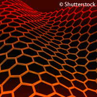
Graphene is a 2D material consisting of a single layer of carbon atoms arranged in a honeycomb or chicken wire structure. It is the thinnest material in the world and yet is also one of the strongest. It conducts electricity as efficiently as copper and outperforms all other materials as a conductor of heat.
The scientists proved that a new side-view imaging technique can be used to visualise the individual atomic layers of graphene within the devices they have built. They found that the structures were almost perfect even when more than 10 different layers were used to build the stack.
This development further proves graphene's suitability as a major component in the next generation of computer chips.
The researchers' side-view imaging approach works by first extracting a thin slice from the centre of the device. The team likens this to cutting through a rock to reveal the geological layers or slicing into a chocolate cake to reveal the individual layers of icing.
The scientists used a beam of ions to cut into the surface of the graphene and dig a trench on either side of the section they wanted to isolate. They then removed a thin slice of the device.
Lead study author Dr Sarah Haigh, from the University of Manchester, comments: 'Our slices are only around 100 atoms thick and this allows us to visualise the individual atomic layers of graphene in projection.
'We have found that the observed roughness of the graphene is correlated with their conductivity. Of course we have to make all our electrical measurements before cutting into the device. We were also able to observe that the layers were perfectly clean and that any debris left over from production segregated into isolated pockets and so did not affect device performance. We plan to use this new side view imaging approach to improve the performance of our graphene devices.'
Two of the study researchers, Andre Geim and Konstantin Novoselov, both from the University of Manchester, were awarded the Nobel Prize in Physics in 2010 for their 'groundbreaking experiments regarding the two-dimensional material graphene'.
####
For more information, please click here
Copyright © Cordis
If you have a comment, please Contact us.Issuers of news releases, not 7th Wave, Inc. or Nanotechnology Now, are solely responsible for the accuracy of the content.
Bookmark:


| Related News Press |
News and information
![]() Simulating magnetization in a Heisenberg quantum spin chain April 5th, 2024
Simulating magnetization in a Heisenberg quantum spin chain April 5th, 2024
![]() NRL charters Navy�s quantum inertial navigation path to reduce drift April 5th, 2024
NRL charters Navy�s quantum inertial navigation path to reduce drift April 5th, 2024
![]() Discovery points path to flash-like memory for storing qubits: Rice find could hasten development of nonvolatile quantum memory April 5th, 2024
Discovery points path to flash-like memory for storing qubits: Rice find could hasten development of nonvolatile quantum memory April 5th, 2024
Imaging
![]() Nanoscale CL thermometry with lanthanide-doped heavy-metal oxide in TEM March 8th, 2024
Nanoscale CL thermometry with lanthanide-doped heavy-metal oxide in TEM March 8th, 2024
Graphene/ Graphite
![]() NRL discovers two-dimensional waveguides February 16th, 2024
NRL discovers two-dimensional waveguides February 16th, 2024
Chip Technology
![]() Discovery points path to flash-like memory for storing qubits: Rice find could hasten development of nonvolatile quantum memory April 5th, 2024
Discovery points path to flash-like memory for storing qubits: Rice find could hasten development of nonvolatile quantum memory April 5th, 2024
![]() Utilizing palladium for addressing contact issues of buried oxide thin film transistors April 5th, 2024
Utilizing palladium for addressing contact issues of buried oxide thin film transistors April 5th, 2024
![]() HKUST researchers develop new integration technique for efficient coupling of III-V and silicon February 16th, 2024
HKUST researchers develop new integration technique for efficient coupling of III-V and silicon February 16th, 2024
Discoveries
![]() Chemical reactions can scramble quantum information as well as black holes April 5th, 2024
Chemical reactions can scramble quantum information as well as black holes April 5th, 2024
![]() New micromaterial releases nanoparticles that selectively destroy cancer cells April 5th, 2024
New micromaterial releases nanoparticles that selectively destroy cancer cells April 5th, 2024
![]() Utilizing palladium for addressing contact issues of buried oxide thin film transistors April 5th, 2024
Utilizing palladium for addressing contact issues of buried oxide thin film transistors April 5th, 2024
Announcements
![]() NRL charters Navy�s quantum inertial navigation path to reduce drift April 5th, 2024
NRL charters Navy�s quantum inertial navigation path to reduce drift April 5th, 2024
![]() Discovery points path to flash-like memory for storing qubits: Rice find could hasten development of nonvolatile quantum memory April 5th, 2024
Discovery points path to flash-like memory for storing qubits: Rice find could hasten development of nonvolatile quantum memory April 5th, 2024
Grants/Sponsored Research/Awards/Scholarships/Gifts/Contests/Honors/Records
![]() Discovery points path to flash-like memory for storing qubits: Rice find could hasten development of nonvolatile quantum memory April 5th, 2024
Discovery points path to flash-like memory for storing qubits: Rice find could hasten development of nonvolatile quantum memory April 5th, 2024
![]() Chemical reactions can scramble quantum information as well as black holes April 5th, 2024
Chemical reactions can scramble quantum information as well as black holes April 5th, 2024
|
|
||
|
|
||
| The latest news from around the world, FREE | ||
|
|
||
|
|
||
| Premium Products | ||
|
|
||
|
Only the news you want to read!
Learn More |
||
|
|
||
|
Full-service, expert consulting
Learn More |
||
|
|
||