Home > Press > Photovoltaics from any semiconductor: Berkeley Lab technology could open door to more widespread solar energy devices
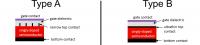 |
| The SFPV technology was tested for two top electrode architectures: (A) the top electrode is shaped into narrow fingers; (B) top electrode is uniformly ultrathin.
Credit: (Image courtesy of Berkeley Lab) |
Abstract:
A technology that would enable low-cost, high efficiency solar cells to be made from virtually any semiconductor material has been developed by researchers with the U.S. Department of Energy (DOE)'s Lawrence Berkeley National Laboratory (Berkeley Lab) and the University of California (UC) Berkeley. This technology opens the door to the use of plentiful, relatively inexpensive semiconductors, such as the promising metal oxides, sulfides and phosphides, that have been considered unsuitable for solar cells because it is so difficult to taylor their properties by chemical means.
Photovoltaics from any semiconductor: Berkeley Lab technology could open door to more widespread solar energy devices
Berkeley, CA | Posted on July 27th, 2012"It's time we put bad materials to good use," says physicist Alex Zettl, who led this research along with colleague Feng Wang. "Our technology allows us to sidestep the difficulty in chemically tailoring many earth abundant, non-toxic semiconductors and instead tailor these materials simply by applying an electric field."
Zettl, who holds joint appointments with Berkeley Lab's Materials Sciences Division and UC Berkeley's Physics Department where he directs the Center of Integrated Nanomechanical Systems (COINS), is the corresponding author of a paper describing this work in the journal Nano Letters. The paper is titled "Screening- Engineered Field-Effect Solar Cells." Co-authoring it were William Regan, Steven Byrnes, Will Gannett, Onur Ergen, Oscar Vazquez-Mena and Feng Wang.
Solar cells convert sunlight into electricity using semiconductor materials that exhibit the photovoltaic effect - meaning they absorb photons and release electrons that can be channeled into an electrical current. Photovoltaics are the ultimate source of clean, green and renewable energy but today's technologies utilize relatively scarce and expensive semiconductors, such as large crystals of silicon, or thin films of cadmium telluride or copper indium gallium selenide, that are tricky or expensive to fabricate into devices.
"Solar technologies today face a cost-to-efficiency trade-off that has slowed widespread implementation," Zettl says. "Our technology reduces the cost and complexity of fabricating solar cells and thereby provides what could be an important cost-effective and environmentally friendly alternative that would accelerate the usage of solar energy."
This new technology is called "screening-engineered field-effect photovoltaics," or SFPV, because it utilizes the electric field effect, a well understood phenomenon by which the concentration of charge-carriers in a semiconductor is altered by the application of an electric field. With the SFPV technology, a carefully designed partially screening top electrode lets the gate electric field sufficiently penetrate the electrode and more uniformly modulate the semiconductor carrier concentration and type to induce a p-n junction. This enables the creation of high quality p-n junctions in semiconductors that are difficult if not impossible to dope by conventional chemical methods.
"Our technology requires only electrode and gate deposition, without the need for high-temperature chemical doping, ion implantation, or other expensive or damaging processes," says lead author William Regan. "The key to our success is the minimal screening of the gate field which is achieved through geometric structuring of the top electrode. This makes it possible for electrical contact to and carrier modulation of the semiconductor to be performed simultaneously."
Under the SFPV system, the architecture of the top electrode is structured so that at least one of the electrode's dimensions is confined. In one configuration, working with copper oxide, the Berkeley researchers shaped the electrode contact into narrow fingers; in another configuration, working with silicon, they made the top contact ultra-thin (single layer graphene) across the surface. With sufficiently narrow fingers, the gate field creates a low electrical resistance inversion layer between the fingers and a potential barrier beneath them. A uniformly thin top contact allows gate fields to penetrate and deplete/invert the underlying semiconductor. The results in both configurations are high quality p-n junctions.
Says co-author Feng Wang, "Our demonstrations show that a stable, electrically contacted p-n junction can be achieved with nearly any semiconductor and any electrode material through the application of a gate field provided that the electrode is appropriately geometrically structured."
The researchers also demonstrated the SFPV effect in a self-gating configuration, in which the gate was powered internally by the electrical activity of the cell itself.
"The self-gating configuration eliminates the need for an external gate power source, which will simplify the practical implementation of SFPV devices," Regan says. "Additionally, the gate can serve a dual role as an antireflection coating, a feature already common and necessary for high efficiency photovoltaics."
This research was supported in part by the DOE Office of Science and in part by the National Science Foundation.
####
About DOE/Lawrence Berkeley National Laboratory
Lawrence Berkeley National Laboratory (Berkeley Lab) addresses the world's most urgent scientific challenges by advancing sustainable energy, protecting human health, creating new materials, and revealing the origin and fate of the universe. Founded in 1931, Berkeley Lab's scientific expertise has been recognized with 13 Nobel prizes. The University of California manages Berkeley Lab for the U.S. Department of Energy's Office of Science. For more, visit www.lbl.gov.
For more information, please click here
Contacts:
Lynn Yarris
510-486-5375
Copyright © DOE/Lawrence Berkeley National Laboratory
If you have a comment, please Contact us.Issuers of news releases, not 7th Wave, Inc. or Nanotechnology Now, are solely responsible for the accuracy of the content.
Bookmark:


| Related News Press |
News and information
![]() Simulating magnetization in a Heisenberg quantum spin chain April 5th, 2024
Simulating magnetization in a Heisenberg quantum spin chain April 5th, 2024
![]() NRL charters Navy�s quantum inertial navigation path to reduce drift April 5th, 2024
NRL charters Navy�s quantum inertial navigation path to reduce drift April 5th, 2024
![]() Discovery points path to flash-like memory for storing qubits: Rice find could hasten development of nonvolatile quantum memory April 5th, 2024
Discovery points path to flash-like memory for storing qubits: Rice find could hasten development of nonvolatile quantum memory April 5th, 2024
Laboratories
![]() A battery�s hopping ions remember where they�ve been: Seen in atomic detail, the seemingly smooth flow of ions through a battery�s electrolyte is surprisingly complicated February 16th, 2024
A battery�s hopping ions remember where they�ve been: Seen in atomic detail, the seemingly smooth flow of ions through a battery�s electrolyte is surprisingly complicated February 16th, 2024
![]() NRL discovers two-dimensional waveguides February 16th, 2024
NRL discovers two-dimensional waveguides February 16th, 2024
![]() Three-pronged approach discerns qualities of quantum spin liquids November 17th, 2023
Three-pronged approach discerns qualities of quantum spin liquids November 17th, 2023
Govt.-Legislation/Regulation/Funding/Policy
![]() NRL charters Navy�s quantum inertial navigation path to reduce drift April 5th, 2024
NRL charters Navy�s quantum inertial navigation path to reduce drift April 5th, 2024
![]() Discovery points path to flash-like memory for storing qubits: Rice find could hasten development of nonvolatile quantum memory April 5th, 2024
Discovery points path to flash-like memory for storing qubits: Rice find could hasten development of nonvolatile quantum memory April 5th, 2024
![]() Chemical reactions can scramble quantum information as well as black holes April 5th, 2024
Chemical reactions can scramble quantum information as well as black holes April 5th, 2024
Discoveries
![]() Chemical reactions can scramble quantum information as well as black holes April 5th, 2024
Chemical reactions can scramble quantum information as well as black holes April 5th, 2024
![]() New micromaterial releases nanoparticles that selectively destroy cancer cells April 5th, 2024
New micromaterial releases nanoparticles that selectively destroy cancer cells April 5th, 2024
![]() Utilizing palladium for addressing contact issues of buried oxide thin film transistors April 5th, 2024
Utilizing palladium for addressing contact issues of buried oxide thin film transistors April 5th, 2024
Announcements
![]() NRL charters Navy�s quantum inertial navigation path to reduce drift April 5th, 2024
NRL charters Navy�s quantum inertial navigation path to reduce drift April 5th, 2024
![]() Discovery points path to flash-like memory for storing qubits: Rice find could hasten development of nonvolatile quantum memory April 5th, 2024
Discovery points path to flash-like memory for storing qubits: Rice find could hasten development of nonvolatile quantum memory April 5th, 2024
Energy
![]() Development of zinc oxide nanopagoda array photoelectrode: photoelectrochemical water-splitting hydrogen production January 12th, 2024
Development of zinc oxide nanopagoda array photoelectrode: photoelectrochemical water-splitting hydrogen production January 12th, 2024
![]() Shedding light on unique conduction mechanisms in a new type of perovskite oxide November 17th, 2023
Shedding light on unique conduction mechanisms in a new type of perovskite oxide November 17th, 2023
![]() Inverted perovskite solar cell breaks 25% efficiency record: Researchers improve cell efficiency using a combination of molecules to address different November 17th, 2023
Inverted perovskite solar cell breaks 25% efficiency record: Researchers improve cell efficiency using a combination of molecules to address different November 17th, 2023
![]() The efficient perovskite cells with a structured anti-reflective layer � another step towards commercialization on a wider scale October 6th, 2023
The efficient perovskite cells with a structured anti-reflective layer � another step towards commercialization on a wider scale October 6th, 2023
Solar/Photovoltaic
![]() Development of zinc oxide nanopagoda array photoelectrode: photoelectrochemical water-splitting hydrogen production January 12th, 2024
Development of zinc oxide nanopagoda array photoelectrode: photoelectrochemical water-splitting hydrogen production January 12th, 2024
![]() Shedding light on unique conduction mechanisms in a new type of perovskite oxide November 17th, 2023
Shedding light on unique conduction mechanisms in a new type of perovskite oxide November 17th, 2023
![]() Inverted perovskite solar cell breaks 25% efficiency record: Researchers improve cell efficiency using a combination of molecules to address different November 17th, 2023
Inverted perovskite solar cell breaks 25% efficiency record: Researchers improve cell efficiency using a combination of molecules to address different November 17th, 2023
![]() Charged �molecular beasts� the basis for new compounds: Researchers at Leipzig University use �aggressive� fragments of molecular ions for chemical synthesis November 3rd, 2023
Charged �molecular beasts� the basis for new compounds: Researchers at Leipzig University use �aggressive� fragments of molecular ions for chemical synthesis November 3rd, 2023
|
|
||
|
|
||
| The latest news from around the world, FREE | ||
|
|
||
|
|
||
| Premium Products | ||
|
|
||
|
Only the news you want to read!
Learn More |
||
|
|
||
|
Full-service, expert consulting
Learn More |
||
|
|
||