Home > Press > JEOL Puts New Spin on NeoScope Benchtop SEM
 |
Abstract:
Since its initial introduction in 2008, the JEOL NeoScope benchtop Scanning Electron Microscope (SEM), represented by Nikon Instruments, has been used for inspection of electronic parts, forensics analysis, pharmaceutical inspection, and imaging insects for student projects. It is also used in conjunction with both optical microscopes and traditional SEMs in the lab.
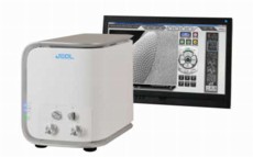
JEOL Puts New Spin on NeoScope Benchtop SEM
San Francisco, CA | Posted on July 10th, 2012Now JEOL introduces the NeoScope with higher magnification, multi-touch screen control, and a sleek new design.
As simple to use as a digital camera, the NeoScope is a high resolution SEM that produces images with a large depth of field at magnifications ranging from 10X - 60,000X. It features both high and low vacuum operation, three selectable accelerating voltages, and secondary electron and backscattered electron imaging. The NeoScope accommodates samples up to 70mm in diameter and 50mm in thickness. Both conductive and non-conductive samples can be examined. Optional EDS is available for elemental analysis.
An additional new feature of the NeoScope SEM is touch screen interface with the familiar look and feel of today's smart phones and touch pads. Automatic functions as well as pre-stored recipe files make it easy to use for a multitude of sample types. Any skill level of user will appreciate the simplicity and fast operation, from sample loading to imaging in vacuum in less than three minutes.
Visit www.nikoninstruments.com or www.jeolusa.com for more information about the NeoScope from JEOL.
####
About JEOL USA, Inc.
JEOL is a world leader in electron optical equipment and instrumentation for high-end scientific and industrial research and development. Core product groups include electron microscopes (SEMs and TEMs), instruments for the semiconductor industry (electron beam lithography and a series of defect review and inspection tools), and analytical instruments including mass spectrometers, NMRs and ESRs.
JEOL USA, Inc., is a wholly owned subsidiary of JEOL, Ltd., Japan, was incorporated in the United States in 1962. The company has 13 regional service centers that offer unlimited emergency service and support in the U.S.
For more information, please click here
Contacts:
Pamela Mansfield
Marketing Communications
JEOL USA
978.536.2309
www.jeolusa.com
Copyright © JEOL USA, Inc.
If you have a comment, please Contact us.Issuers of news releases, not 7th Wave, Inc. or Nanotechnology Now, are solely responsible for the accuracy of the content.
Bookmark:


| Related News Press |
News and information
![]() Simulating magnetization in a Heisenberg quantum spin chain April 5th, 2024
Simulating magnetization in a Heisenberg quantum spin chain April 5th, 2024
![]() NRL charters Navy�s quantum inertial navigation path to reduce drift April 5th, 2024
NRL charters Navy�s quantum inertial navigation path to reduce drift April 5th, 2024
![]() Discovery points path to flash-like memory for storing qubits: Rice find could hasten development of nonvolatile quantum memory April 5th, 2024
Discovery points path to flash-like memory for storing qubits: Rice find could hasten development of nonvolatile quantum memory April 5th, 2024
Imaging
![]() Nanoscale CL thermometry with lanthanide-doped heavy-metal oxide in TEM March 8th, 2024
Nanoscale CL thermometry with lanthanide-doped heavy-metal oxide in TEM March 8th, 2024
![]() The USTC realizes In situ electron paramagnetic resonance spectroscopy using single nanodiamond sensors November 3rd, 2023
The USTC realizes In situ electron paramagnetic resonance spectroscopy using single nanodiamond sensors November 3rd, 2023
![]() Observation of left and right at nanoscale with optical force October 6th, 2023
Observation of left and right at nanoscale with optical force October 6th, 2023
Announcements
![]() NRL charters Navy�s quantum inertial navigation path to reduce drift April 5th, 2024
NRL charters Navy�s quantum inertial navigation path to reduce drift April 5th, 2024
![]() Discovery points path to flash-like memory for storing qubits: Rice find could hasten development of nonvolatile quantum memory April 5th, 2024
Discovery points path to flash-like memory for storing qubits: Rice find could hasten development of nonvolatile quantum memory April 5th, 2024
Tools
![]() Ferroelectrically modulate the Fermi level of graphene oxide to enhance SERS response November 3rd, 2023
Ferroelectrically modulate the Fermi level of graphene oxide to enhance SERS response November 3rd, 2023
![]() The USTC realizes In situ electron paramagnetic resonance spectroscopy using single nanodiamond sensors November 3rd, 2023
The USTC realizes In situ electron paramagnetic resonance spectroscopy using single nanodiamond sensors November 3rd, 2023
Events/Classes
![]() Researchers demonstrate co-propagation of quantum and classical signals: Study shows that quantum encryption can be implemented in existing fiber networks January 20th, 2023
Researchers demonstrate co-propagation of quantum and classical signals: Study shows that quantum encryption can be implemented in existing fiber networks January 20th, 2023
|
|
||
|
|
||
| The latest news from around the world, FREE | ||
|
|
||
|
|
||
| Premium Products | ||
|
|
||
|
Only the news you want to read!
Learn More |
||
|
|
||
|
Full-service, expert consulting
Learn More |
||
|
|
||