Home > Press > Taming light with graphene: Scientists visualize the trapping and confinement of light on graphene, making a sheet of carbon atoms the most promising candidate for optical information processing on the nano-scale, optical detection, and ultrafast optoelectronics
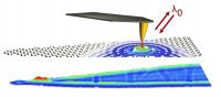 |
| This image shows optical nanoimaging of graphene plasmons. The upper panel shows a sketch of the imaging method. A laser illuminated scanning tip launches plasmons on graphene. Detection is by recording the light backscattered from the tip. The lower panel shows optical image of graphene, where the fringes visualize the interference of the graphene plasmons.
Credit: nanoGUNE, IQFR-CSIC, ICFO |
Abstract:
Spanish research groups achieve first ever visualizations of light guided with nanometric precision on graphene (a one-atom-thick sheet of carbon atoms). This visualization proves what theoretical physicists have long predicted; that it is possible to trap and manipulate light in a highly efficient way, using graphene as a novel platform for optical information processing and sensing. Synergies between theoretical proposals from IQFR-CSIC (Madrid), specializations in graphene nano-photonics and nano-optoelectonics at ICFO (Barcelona), and experimental expertise in optical nano-imaging at nanoGUNE (San Sebastian) give rise to these noteworthy results reported in Nature this week in a back-to-back publication alongside a similar study by the group of Dmitry Basov in UCSD in California.
Taming light with graphene: Scientists visualize the trapping and confinement of light on graphene, making a sheet of carbon atoms the most promising candidate for optical information processing on the nano-scale, optical detection, and ultrafast optoelectronics
Spain | Posted on June 20th, 2012Graphene is a material that, among many other fascinating properties, has an extraordinary optical behavior. Particularly interesting optical properties had been predicted for the case that light couples to so-called plasmons, wave-like excitations that were predicted to exist in the "sea" of conduction electrons of graphene. However, no direct experimental evidence of plasmons in graphene had been shown up to this work. This is because the wavelength of graphene plasmons is 10 to 100 times smaller than what can be seen with conventional light microscopes. Now, the researchers show the first experimental images of graphene plasmons. They used a so called near-field microscope that uses a sharp tip to convert the illumination light into a nanoscale light spot that provides the extra push needed for the plasmons to be created. At the same time the tip probes the presence of plasmons (see figure). Rainer Hillenbrand, leader of the nanoGUNE group comments: "Seeing is believing! Our near-field optical images definitely proof the existence of propagating and localized graphene plasmons and allow for a direct measurement of their dramatically reduced wavelength."
As demonstrated by the researchers, graphene plasmons can be used to electrically control light in a similar fashion as is traditionally achieved with electrons in a transistor. These capabilities, which until now were impossible with other existing plasmonic materials, enable new highly efficient nano-scale optical switches which can perform calculations using light instead of electricity. "With our work we show that graphene is an excellent choice for solving the long-standing and technologically important problem of modulating light at the speeds of today's microchips," says Javier Garc�a de Abajo, leader of the IQFR-CSIC group. In addition, the capability of trapping light in very small volumes could give rise to a new generation of nano-sensors with applications in diverse areas such as medicine and bio-detection, solar cells and light detectors, as well as quantum information processing. This result literally opens a new field of research and provides a first viable path towards ultrafast tuning of light, which was not possible until now. Frank Koppens, leader of the ICFO group, summarizes: "Graphene is a novel and unique material for plasmonics, truly bridging the fields of nano-electronics and nano-optics".
###
Published manuscript:
Optical nano-imaging of gate-tunable graphene plasmons Jianing Chen, Michela Badioli, Pablo Alonso-Gonz�lez, Susokin Thongrattanasiri, Florian Huth, Johann Osmond, Marko Spasenović, Alba Centeno, Amaia Pesquera, Philippe Godignon, Amaia Zurutuza, Nicolas Camara, Javier Garc�a de Abajo, Rainer Hillenbrand & Frank Koppens
DOI: 10.1038/nature11254
Contributions and institutes:
Optical nano-imaging: CIC nanoGUNE Consolider (San Sebastian, Spain), CFM-CSIC-UPV/EHU (San Sebastian, Spain), Neaspec GmbH (Martinsried, Germany), Ikerbasque (Bilbao, Spain)
Graphene nano-photonics and optoelectronics: ICFO (Barcelona, Spain)
Theory: IQFR-CSIC (Madrid, Spain)
Graphene synthesis: Graphenea (San Sebastian, Spain) University of Tours (Tours, France), and CNM-IMB-CSIC (Barcelona, Spain)
####
For more information, please click here
Contacts:
Aitziber Lasa Iglesias
34-943-363-040
Copyright © Elhuyar Fundazioa
If you have a comment, please Contact us.Issuers of news releases, not 7th Wave, Inc. or Nanotechnology Now, are solely responsible for the accuracy of the content.
Bookmark:


| Related News Press |
News and information
![]() Simulating magnetization in a Heisenberg quantum spin chain April 5th, 2024
Simulating magnetization in a Heisenberg quantum spin chain April 5th, 2024
![]() NRL charters Navy�s quantum inertial navigation path to reduce drift April 5th, 2024
NRL charters Navy�s quantum inertial navigation path to reduce drift April 5th, 2024
![]() Discovery points path to flash-like memory for storing qubits: Rice find could hasten development of nonvolatile quantum memory April 5th, 2024
Discovery points path to flash-like memory for storing qubits: Rice find could hasten development of nonvolatile quantum memory April 5th, 2024
Imaging
![]() Nanoscale CL thermometry with lanthanide-doped heavy-metal oxide in TEM March 8th, 2024
Nanoscale CL thermometry with lanthanide-doped heavy-metal oxide in TEM March 8th, 2024
Graphene/ Graphite
![]() NRL discovers two-dimensional waveguides February 16th, 2024
NRL discovers two-dimensional waveguides February 16th, 2024
Chip Technology
![]() Discovery points path to flash-like memory for storing qubits: Rice find could hasten development of nonvolatile quantum memory April 5th, 2024
Discovery points path to flash-like memory for storing qubits: Rice find could hasten development of nonvolatile quantum memory April 5th, 2024
![]() Utilizing palladium for addressing contact issues of buried oxide thin film transistors April 5th, 2024
Utilizing palladium for addressing contact issues of buried oxide thin film transistors April 5th, 2024
![]() HKUST researchers develop new integration technique for efficient coupling of III-V and silicon February 16th, 2024
HKUST researchers develop new integration technique for efficient coupling of III-V and silicon February 16th, 2024
Quantum Computing
![]() Simulating magnetization in a Heisenberg quantum spin chain April 5th, 2024
Simulating magnetization in a Heisenberg quantum spin chain April 5th, 2024
![]() Discovery points path to flash-like memory for storing qubits: Rice find could hasten development of nonvolatile quantum memory April 5th, 2024
Discovery points path to flash-like memory for storing qubits: Rice find could hasten development of nonvolatile quantum memory April 5th, 2024
![]() With VECSELs towards the quantum internet Fraunhofer: IAF achieves record output power with VECSEL for quantum frequency converters April 5th, 2024
With VECSELs towards the quantum internet Fraunhofer: IAF achieves record output power with VECSEL for quantum frequency converters April 5th, 2024
![]() Chemical reactions can scramble quantum information as well as black holes April 5th, 2024
Chemical reactions can scramble quantum information as well as black holes April 5th, 2024
Optical computing/Photonic computing
![]() With VECSELs towards the quantum internet Fraunhofer: IAF achieves record output power with VECSEL for quantum frequency converters April 5th, 2024
With VECSELs towards the quantum internet Fraunhofer: IAF achieves record output power with VECSEL for quantum frequency converters April 5th, 2024
![]() Chemical reactions can scramble quantum information as well as black holes April 5th, 2024
Chemical reactions can scramble quantum information as well as black holes April 5th, 2024
![]() Optically trapped quantum droplets of light can bind together to form macroscopic complexes March 8th, 2024
Optically trapped quantum droplets of light can bind together to form macroscopic complexes March 8th, 2024
![]() HKUST researchers develop new integration technique for efficient coupling of III-V and silicon February 16th, 2024
HKUST researchers develop new integration technique for efficient coupling of III-V and silicon February 16th, 2024
Sensors
Discoveries
![]() Chemical reactions can scramble quantum information as well as black holes April 5th, 2024
Chemical reactions can scramble quantum information as well as black holes April 5th, 2024
![]() New micromaterial releases nanoparticles that selectively destroy cancer cells April 5th, 2024
New micromaterial releases nanoparticles that selectively destroy cancer cells April 5th, 2024
![]() Utilizing palladium for addressing contact issues of buried oxide thin film transistors April 5th, 2024
Utilizing palladium for addressing contact issues of buried oxide thin film transistors April 5th, 2024
Announcements
![]() NRL charters Navy�s quantum inertial navigation path to reduce drift April 5th, 2024
NRL charters Navy�s quantum inertial navigation path to reduce drift April 5th, 2024
![]() Discovery points path to flash-like memory for storing qubits: Rice find could hasten development of nonvolatile quantum memory April 5th, 2024
Discovery points path to flash-like memory for storing qubits: Rice find could hasten development of nonvolatile quantum memory April 5th, 2024
Tools
![]() Ferroelectrically modulate the Fermi level of graphene oxide to enhance SERS response November 3rd, 2023
Ferroelectrically modulate the Fermi level of graphene oxide to enhance SERS response November 3rd, 2023
![]() The USTC realizes In situ electron paramagnetic resonance spectroscopy using single nanodiamond sensors November 3rd, 2023
The USTC realizes In situ electron paramagnetic resonance spectroscopy using single nanodiamond sensors November 3rd, 2023
Photonics/Optics/Lasers
![]() With VECSELs towards the quantum internet Fraunhofer: IAF achieves record output power with VECSEL for quantum frequency converters April 5th, 2024
With VECSELs towards the quantum internet Fraunhofer: IAF achieves record output power with VECSEL for quantum frequency converters April 5th, 2024
![]() Nanoscale CL thermometry with lanthanide-doped heavy-metal oxide in TEM March 8th, 2024
Nanoscale CL thermometry with lanthanide-doped heavy-metal oxide in TEM March 8th, 2024
![]() Optically trapped quantum droplets of light can bind together to form macroscopic complexes March 8th, 2024
Optically trapped quantum droplets of light can bind together to form macroscopic complexes March 8th, 2024
![]() HKUST researchers develop new integration technique for efficient coupling of III-V and silicon February 16th, 2024
HKUST researchers develop new integration technique for efficient coupling of III-V and silicon February 16th, 2024
Research partnerships
![]() Discovery points path to flash-like memory for storing qubits: Rice find could hasten development of nonvolatile quantum memory April 5th, 2024
Discovery points path to flash-like memory for storing qubits: Rice find could hasten development of nonvolatile quantum memory April 5th, 2024
![]() Researchers� approach may protect quantum computers from attacks March 8th, 2024
Researchers� approach may protect quantum computers from attacks March 8th, 2024
![]() 'Sudden death' of quantum fluctuations defies current theories of superconductivity: Study challenges the conventional wisdom of superconducting quantum transitions January 12th, 2024
'Sudden death' of quantum fluctuations defies current theories of superconductivity: Study challenges the conventional wisdom of superconducting quantum transitions January 12th, 2024
Solar/Photovoltaic
![]() Development of zinc oxide nanopagoda array photoelectrode: photoelectrochemical water-splitting hydrogen production January 12th, 2024
Development of zinc oxide nanopagoda array photoelectrode: photoelectrochemical water-splitting hydrogen production January 12th, 2024
![]() Shedding light on unique conduction mechanisms in a new type of perovskite oxide November 17th, 2023
Shedding light on unique conduction mechanisms in a new type of perovskite oxide November 17th, 2023
![]() Inverted perovskite solar cell breaks 25% efficiency record: Researchers improve cell efficiency using a combination of molecules to address different November 17th, 2023
Inverted perovskite solar cell breaks 25% efficiency record: Researchers improve cell efficiency using a combination of molecules to address different November 17th, 2023
![]() Charged �molecular beasts� the basis for new compounds: Researchers at Leipzig University use �aggressive� fragments of molecular ions for chemical synthesis November 3rd, 2023
Charged �molecular beasts� the basis for new compounds: Researchers at Leipzig University use �aggressive� fragments of molecular ions for chemical synthesis November 3rd, 2023
|
|
||
|
|
||
| The latest news from around the world, FREE | ||
|
|
||
|
|
||
| Premium Products | ||
|
|
||
|
Only the news you want to read!
Learn More |
||
|
|
||
|
Full-service, expert consulting
Learn More |
||
|
|
||