Home > Press > Two-Dimensional Layered Materials for High-Performance Electronics
 |
Abstract:
Graphene is the wonder material that could solve the problem of making ever faster computers and smaller mobile devices when current silicon microchip technology hits an inevitable wall. Graphene, a single layer of carbon atoms in a tight hexagonal arrangement, is a highly researched material due to its incredible electronic properties, with theoretical speeds 100 times greater than silicon. But putting the material into a microchip that could outperform current silicon technology has proven difficult.
Two-Dimensional Layered Materials for High-Performance Electronics
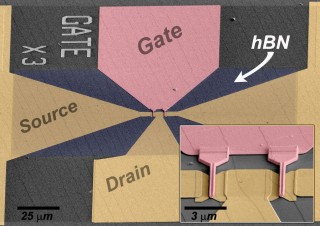
University Park, PA | Posted on May 23rd, 2012The answer may lie in new nanoscale systems based on ultrathin layers of materials with exotic properties. Called two-dimensional layered materials, these systems could be important for microelectronics, various types of hypersensitive sensors, catalysis, tissue engineering and energy storage. Researchers at Penn State have applied one such 2D layered material, a combination of graphene and hexagonal boron nitride, to produce improved transistor performance at an industrially relevant scale.
"Other groups have shown that graphene on boron nitride can improve performance two to three times, but not in a way that could be scaled up. For the first time, we have been able to take this material and apply it to make transistors at wafer scale," says Joshua Robinson, assistant professor of materials science and engineering at Penn State and the corresponding author on a paper reporting their work in the online version of the journal ACS Nano.
In the article, the Penn State team describes a method for integrating a thin layer of graphene only one or two atoms thick, with a second layer of hexagonal boron nitride (hBN) with a thickness of a few atoms up to several hundred atoms. The resulting bilayer material constitutes the next step in creating functional graphene field effect transistors for high frequency electronic and optoelectronic devices.
Previous research by other groups has shown that a common material called hexagonal boron nitride (hBN), a synthetic mixture of boron and nitrogen that is used as an industrial lubricant and is found in many cosmetics, is a potential replacement for silicon dioxide and other high-performance dielectrics that have failed to integrate well with graphene. Because boron sits next to carbon on the periodic table, and hexagonal boron nitride has a similar arrangement of atoms as graphene, the two materials match up well electronically. In fact, hBN is often referred to as white graphene. To be of more than academic interest in the lab, however, the hBN-graphene bilayer had to be grown at wafer scale - from around 3 inches (75 mm) to almost 12 inches (300 mm).
The Penn State team solved this problem by using a prior technique developed in their lab to produce a uniform, large-area, and high quality layer of epitaxial graphene suitable for high frequency applications. This "quasi-freestanding epitaxial graphene" was produced by attaching hydrogen atoms to the graphene in order to "passivate dangling bonds," essentially flattening and smoothing the graphene film. The hexagonal boron nitride was then grown on a transition metal substrate using a chemical vapor deposition technique that is standard in manufacturing. The hBN was released from the substrate via one of several transfer processes and layered on top of the graphene on a 75mm wafer, marking the first integration of epitaxial graphene with hBN on a scale compatible with industry needs.
Building on their earlier work with epitaxial graphene, which had already increased transistor performance by 2-3 times, this research adds a further 2-3x improvement in performance and shows the strong potential for utilizing graphene in electronics, according to Robinson. In the near future, the Penn State team hopes to demonstrate graphene based integrated circuits and high-performance devices suitable for industrial-scale manufacturing on 100mm wafers.
"We use all standard lithography, which is important for nanomanufacturing," Robinson adds. In order to make a dent in the highly competitive microchip industry, a new material system needs to be compatible with current processing technology as well as offer a significant performance boost.
Boron nitride-graphene is one of several up-and-coming two-dimensional layered systems whose nanoscale properties are only beginning to be discovered. Dimensionality, according to Nobel Laureates Novoselov and Geim, is one of the most defining material parameters and can give rise to dramatically different properties according to whether the material structure is 0D, 1D, 2D, or 3D. Penn State is among the pioneers moving into what may prove to be a new frontier of materials science.
In addition to Robinson, the co-authors on the ACS Nano article are Michael Bresnehan, Matthew Hollander, Maxwell Wetherington, Michael LaBella, Kathleen Trumbull, Randal Cavalero, and David Snyder, all of Penn State. The work was supported by the Naval Surface Warfare Center Crane, and instrumentation support was provided by the National Nanotechnology Infrastructure Network at Penn State. "Integration of Hexagonal Boron Nitride with Quasi-freestanding Epitaxial Graphene: Toward Wafer-Scale High-Performance Devices" was published in online in the April 28, 2012, ASAP (as soon as publishable) edition of ACS Nano. Contact Joshua Robinson at .
####
For more information, please click here
Contacts:
Joshua Robinson
Copyright © Newswise
If you have a comment, please Contact us.Issuers of news releases, not 7th Wave, Inc. or Nanotechnology Now, are solely responsible for the accuracy of the content.
Bookmark:


| Related News Press |
News and information
![]() Simulating magnetization in a Heisenberg quantum spin chain April 5th, 2024
Simulating magnetization in a Heisenberg quantum spin chain April 5th, 2024
![]() NRL charters Navy�s quantum inertial navigation path to reduce drift April 5th, 2024
NRL charters Navy�s quantum inertial navigation path to reduce drift April 5th, 2024
![]() Discovery points path to flash-like memory for storing qubits: Rice find could hasten development of nonvolatile quantum memory April 5th, 2024
Discovery points path to flash-like memory for storing qubits: Rice find could hasten development of nonvolatile quantum memory April 5th, 2024
Chemistry
![]() What heat can tell us about battery chemistry: using the Peltier effect to study lithium-ion cells March 8th, 2024
What heat can tell us about battery chemistry: using the Peltier effect to study lithium-ion cells March 8th, 2024
![]() Nanoscale CL thermometry with lanthanide-doped heavy-metal oxide in TEM March 8th, 2024
Nanoscale CL thermometry with lanthanide-doped heavy-metal oxide in TEM March 8th, 2024
Graphene/ Graphite
![]() NRL discovers two-dimensional waveguides February 16th, 2024
NRL discovers two-dimensional waveguides February 16th, 2024
Chip Technology
![]() Discovery points path to flash-like memory for storing qubits: Rice find could hasten development of nonvolatile quantum memory April 5th, 2024
Discovery points path to flash-like memory for storing qubits: Rice find could hasten development of nonvolatile quantum memory April 5th, 2024
![]() Utilizing palladium for addressing contact issues of buried oxide thin film transistors April 5th, 2024
Utilizing palladium for addressing contact issues of buried oxide thin film transistors April 5th, 2024
![]() HKUST researchers develop new integration technique for efficient coupling of III-V and silicon February 16th, 2024
HKUST researchers develop new integration technique for efficient coupling of III-V and silicon February 16th, 2024
Nanomedicine
![]() New micromaterial releases nanoparticles that selectively destroy cancer cells April 5th, 2024
New micromaterial releases nanoparticles that selectively destroy cancer cells April 5th, 2024
![]() Good as gold - improving infectious disease testing with gold nanoparticles April 5th, 2024
Good as gold - improving infectious disease testing with gold nanoparticles April 5th, 2024
![]() Researchers develop artificial building blocks of life March 8th, 2024
Researchers develop artificial building blocks of life March 8th, 2024
Sensors
Discoveries
![]() Chemical reactions can scramble quantum information as well as black holes April 5th, 2024
Chemical reactions can scramble quantum information as well as black holes April 5th, 2024
![]() New micromaterial releases nanoparticles that selectively destroy cancer cells April 5th, 2024
New micromaterial releases nanoparticles that selectively destroy cancer cells April 5th, 2024
![]() Utilizing palladium for addressing contact issues of buried oxide thin film transistors April 5th, 2024
Utilizing palladium for addressing contact issues of buried oxide thin film transistors April 5th, 2024
Announcements
![]() NRL charters Navy�s quantum inertial navigation path to reduce drift April 5th, 2024
NRL charters Navy�s quantum inertial navigation path to reduce drift April 5th, 2024
![]() Discovery points path to flash-like memory for storing qubits: Rice find could hasten development of nonvolatile quantum memory April 5th, 2024
Discovery points path to flash-like memory for storing qubits: Rice find could hasten development of nonvolatile quantum memory April 5th, 2024
Battery Technology/Capacitors/Generators/Piezoelectrics/Thermoelectrics/Energy storage
![]() What heat can tell us about battery chemistry: using the Peltier effect to study lithium-ion cells March 8th, 2024
What heat can tell us about battery chemistry: using the Peltier effect to study lithium-ion cells March 8th, 2024
![]() A battery�s hopping ions remember where they�ve been: Seen in atomic detail, the seemingly smooth flow of ions through a battery�s electrolyte is surprisingly complicated February 16th, 2024
A battery�s hopping ions remember where they�ve been: Seen in atomic detail, the seemingly smooth flow of ions through a battery�s electrolyte is surprisingly complicated February 16th, 2024
|
|
||
|
|
||
| The latest news from around the world, FREE | ||
|
|
||
|
|
||
| Premium Products | ||
|
|
||
|
Only the news you want to read!
Learn More |
||
|
|
||
|
Full-service, expert consulting
Learn More |
||
|
|
||