Home > Press > NanoInk Announces Availability of High Density Tip Arrays for Polymer Pen Lithography: Allows for high-throughput deposition of molecules with well-controlled feature size
 |
Abstract:
NanoInk announced today the availability of High Density (HD) Tip Arrays for Polymer Pen Lithography (PPL). These high-density elastomeric pen arrays are ideal for high-throughput deposition of ink materials. Similar to standard Dip Pen Nanolithography (DPN) with regular silicon nitride pens, High Density Tip Arrays can be used for the deposition of molecules with well-controlled feature size.
NanoInk Announces Availability of High Density Tip Arrays for Polymer Pen Lithography: Allows for high-throughput deposition of molecules with well-controlled feature size
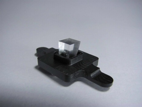
Chicago, IL | Posted on May 1st, 2012High Density Tip Arrays used for Polymer Pen Lithography can easily accommodate several thousands to millions of pens in the same array and are available in a range of array sizes (from 5x5 to 25x25 mm2) with different pen-to-pen pitches (from several microns to hundreds of microns pitch). The versatility of these arrays enables different types of applications in the fields of cell engineering, drug discovery, genomics and materials science.
"When integrated with the 2D leveling mechanism and the large range stage translation of the NLP 2000 System, the HD Tip Array becomes an extremely powerful tool for large scale and high throughput deposition," said Tom Warwick, general manager of NanoInk's NanoFabrication Systems Division. "With the release of HD Tip Array for PPL, we have enhanced our robust scalable nanofabrication offerings, following the earlier release of the NLP 2000 System in 2009 and 1 and 2D leveling in 2011."
NanoInk has devised a proprietary technique for the reliable fabrication of ultra-flat HD Tip Arrays, which can be customized around customer's application requirements. A recent video demonstrating the capability of HD Tip Arrays for PPL is available on NanoInkTV on YouTube. For inquiries about NanoInk's HD Tip Array offerings and customization, please contact Tom Warwick at NanoInk at (847)679-8807 or at .
####
About NanoInk
NanoInk, Inc. is an emerging growth technology company specializing in nanometer-scale manufacturing and applications development for the life sciences, engineering, pharmaceutical, and education industries. Using Dip Pen Nanolithography (DPN) patented and proprietary nanofabrication technology, scientists are enabled to rapidly and easily create micro-and nanoscale structures from a variety of materials on a range of substrates. This low cost, easy to use and scalable technique brings sophisticated nanofabrication to the laboratory desktop. Headquartered in the Illinois Science + Technology Park, north of Chicago, NanoInk currently has several divisions including the NanoFabrication Systems Division, the Nano BioDiscovery Division, the NanoProfessor Division and the NanoGuardian Division.�
NanoInk, the NanoInk logo, Dip Pen Nanolithography, and DPN are registered trademarks of NanoInk, Inc.
For more information, please click here
Contacts:
Joshua Taustein
Dresner Corporate Services
(312)780-7219
David Gutierrez
Dresner Corporate Services
(312)780-7204
Copyright © NanoInk
If you have a comment, please Contact us.Issuers of news releases, not 7th Wave, Inc. or Nanotechnology Now, are solely responsible for the accuracy of the content.
Bookmark:


| Related News Press |
News and information
![]() Simulating magnetization in a Heisenberg quantum spin chain April 5th, 2024
Simulating magnetization in a Heisenberg quantum spin chain April 5th, 2024
![]() NRL charters Navy�s quantum inertial navigation path to reduce drift April 5th, 2024
NRL charters Navy�s quantum inertial navigation path to reduce drift April 5th, 2024
![]() Discovery points path to flash-like memory for storing qubits: Rice find could hasten development of nonvolatile quantum memory April 5th, 2024
Discovery points path to flash-like memory for storing qubits: Rice find could hasten development of nonvolatile quantum memory April 5th, 2024
Announcements
![]() NRL charters Navy�s quantum inertial navigation path to reduce drift April 5th, 2024
NRL charters Navy�s quantum inertial navigation path to reduce drift April 5th, 2024
![]() Discovery points path to flash-like memory for storing qubits: Rice find could hasten development of nonvolatile quantum memory April 5th, 2024
Discovery points path to flash-like memory for storing qubits: Rice find could hasten development of nonvolatile quantum memory April 5th, 2024
Tools
![]() Ferroelectrically modulate the Fermi level of graphene oxide to enhance SERS response November 3rd, 2023
Ferroelectrically modulate the Fermi level of graphene oxide to enhance SERS response November 3rd, 2023
![]() The USTC realizes In situ electron paramagnetic resonance spectroscopy using single nanodiamond sensors November 3rd, 2023
The USTC realizes In situ electron paramagnetic resonance spectroscopy using single nanodiamond sensors November 3rd, 2023
Printing/Lithography/Inkjet/Inks/Bio-printing/Dyes
![]() Presenting: Ultrasound-based printing of 3D materials�potentially inside the body December 8th, 2023
Presenting: Ultrasound-based printing of 3D materials�potentially inside the body December 8th, 2023
![]() Simple ballpoint pen can write custom LEDs August 11th, 2023
Simple ballpoint pen can write custom LEDs August 11th, 2023
![]() Disposable electronics on a simple sheet of paper October 7th, 2022
Disposable electronics on a simple sheet of paper October 7th, 2022
|
|
||
|
|
||
| The latest news from around the world, FREE | ||
|
|
||
|
|
||
| Premium Products | ||
|
|
||
|
Only the news you want to read!
Learn More |
||
|
|
||
|
Full-service, expert consulting
Learn More |
||
|
|
||