Home > Press > Better Organic Electronics: Berkeley Lab Researchers Show the Way Forward for Improving Organic and Molecular Electronic Devices
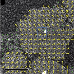 |
| Scanning transmission electron microscopy image of an organic thin film deposited on a silicon nitride membrane. Yellow arrows indicate the lattice orientation of each crystalline domain. Green circles mark polycrystalline areas. (Image from Berkeley Lab�s Molecular Foundry) |
Abstract:
Future prospects for superior new organic electronic devices are brighter now thanks to a new study by researchers with the U.S. Department of Energy (DOE)'s Lawrence Berkeley National Laboratory (Berkeley Lab). Working at the Lab's Molecular Foundry, a DOE nanoscience center, the team has provided the first experimental determination of the pathways by which electrical charge is transported from molecule-to-molecule in an organic thin film. Their results also show how such organic films can be chemically modified to improve conductance.
Better Organic Electronics: Berkeley Lab Researchers Show the Way Forward for Improving Organic and Molecular Electronic Devices
Berkeley, CA | Posted on March 20th, 2012"We have shown that when the molecules in organic thin films are aligned in particular directions, there is much better conductance," says Miquel Salmeron, a leading authority on nanoscale surface imaging who directs Berkeley Lab's Materials Sciences Division and who led this study. "Chemists already know how to fabricate organic thin films in a way that can achieve such an alignment, which means they should be able to use the information provided by our methodology to determine the molecular alignment and its role on charge transport across and along the molecules. This will help improve the performances of future organic electronic devices."
Salmeron and Shaul Aloni, also of the Materials Sciences Division, are the corresponding authors of a paper in the journal NanoLetters that describes this work. The paper is titled "Electron Microscopy Reveals Structure and Morphology of One Molecule Thin Organic Films." Other co-authors were Virginia Altoe, Florent Martin and Allard Katan.
Organic electronics, also known as plastic or polymer electronics, are devices that utilize carbon-based molecules as conductors rather than metals or semiconductors. They are prized for their low costs, light weight and rubbery flexibility. Organic electronics are also expected to play a big role in molecular computing, but to date their use has been hampered by low electrical conductance in comparison to metals and semiconductors.
"Chemists and engineers have been using their intuition and trial-and-error testing to make progress in the field but at some point you hit a wall unless you understand what is going on at the molecular level, for example, how electrons or holes flow through or across molecules, how the charge transport depends on the structure of the organic layers and the orientation of the molecules, and how the charge transport responds to mechanical forces and chemical inputs," Salmeron says. "With our experimental results, we have shown that we can now provide answers for these questions."
In this study, Salmeron and his colleagues used electron diffraction patterns to map the crystal structures of molecular films made from monolayers of short versions of commonly used polymers containing long chains of thiophene units. They focused specifically on pentathiophene butyric acid (5TBA) and two of its derivatives (D5TBA and DH5TBA) that were induced to self-assemble on various electron-transparent substrates. Pentathiophenes - molecules containing a ring of four carbon and one sulfur atoms - are members of a well-studied and promising family of organic semiconductors.
Obtaining structural crystallographic maps of monolayer organic films using electron beams posed a major challenge, as Aloni explains.
"These organic molecules are extremely sensitive to high energy electrons," he says. "When you shoot a beam of high energy electrons through the film it immediately affects the molecules. Within few seconds we no longer see the signature intermolecular alignment of the diffraction pattern. Despite this, when applied correctly, electron microscopy becomes essential tool that can provide unique information on organic samples."
Salmeron, Aloni and their colleagues overcame the challenge through the combination of a unique strategy they developed and a transmission electron microscope (TEM) at the Molecular Foundry's Imaging and Manipulation of Nanostructures Facility. Electron diffraction patterns were collected as a parallel electron beam was scanned over the film, then analyzed by computer to generate structural crystallographic maps.
"These maps contain uncompromised information of the size, symmetry and orientation of the unit cell, the orientation and structure of the domains, the degree of crystallinity, and any variations on the micrometer scale," says first author Altoe. "Such data are crucial to understanding the structure and electrical transport properties of the organic films, and allow us to track small changes driven by chemical modifications of the support films."
In their paper, the authors acknowledge that to gain structural information they had to sacrifice some resolution.
"The achievable resolution of the structural map is a compromise between sample radiation hardness, detector sensitivity and noise, and data acquisition rate," Salmeron says. "To keep the dose of high energy electrons at a level the monolayer film could support and still be able to collect valuable information about its structure, we had to spread the beam to a 90 nanometer diameter. However a fast and direct control of the beam position combined with the use of fast and ultrasensitive detectors should allow for the use of smaller beams with a higher electron flux, resulting in a better than 10 nanometer resolution."
While the combination of organic molecular films and substrates in this study conduct electrical current via electron holes (positively-charged energy spaces), Salmeron and his colleagues say their structural mapping can also be applied to materials whose conductance is electron-based.
"We expect our methodology to have widespread applications in materials research," Salmeron says.
Aloni and Altoe say this methodology is now available at the Imaging and Manipulation of Nanostructures Facility for users of the Molecular Foundry.
This research was supported by the DOE Office of Science.
####
About Berkeley Lab
Lawrence Berkeley National Laboratory addresses the world�s most urgent scientific challenges by advancing sustainable energy, protecting human health, creating new materials, and revealing the origin and fate of the universe. Founded in 1931, Berkeley Lab�s scientific expertise has been recognized with 13 Nobel prizes. The University of California manages Berkeley Lab for the U.S. Department of Energy�s Office of Science. For more, visit www.lbl.gov.
The Molecular Foundry is one of five DOE Nanoscale Science Research Centers (NSRCs), national user facilities for interdisciplinary research at the nanoscale, supported by the DOE Office of Science. Together the NSRCs comprise a suite of complementary facilities that provide researchers with state-of-the-art capabilities to fabricate, process, characterize and model nanoscale materials, and constitute the largest infrastructure investment of the National Nanotechnology Initiative. The NSRCs are located at DOE�s Argonne, Brookhaven, Lawrence Berkeley, Oak Ridge and Sandia and Los Alamos National Laboratories. For more information about the DOE NSRCs, please visit science.energy.gov.
For more information, please click here
Contacts:
Lynn Yarris
(510) 486-5375
Copyright © Berkeley Lab
If you have a comment, please Contact us.Issuers of news releases, not 7th Wave, Inc. or Nanotechnology Now, are solely responsible for the accuracy of the content.
Bookmark:


| Related Links |
![]() For more about the research of Miquel Salmeron, go here:
For more about the research of Miquel Salmeron, go here:
![]() For more about the Molecular Foundry, go here:
For more about the Molecular Foundry, go here:
| Related News Press |
News and information
![]() Simulating magnetization in a Heisenberg quantum spin chain April 5th, 2024
Simulating magnetization in a Heisenberg quantum spin chain April 5th, 2024
![]() NRL charters Navy�s quantum inertial navigation path to reduce drift April 5th, 2024
NRL charters Navy�s quantum inertial navigation path to reduce drift April 5th, 2024
![]() Discovery points path to flash-like memory for storing qubits: Rice find could hasten development of nonvolatile quantum memory April 5th, 2024
Discovery points path to flash-like memory for storing qubits: Rice find could hasten development of nonvolatile quantum memory April 5th, 2024
![]() Good as gold - improving infectious disease testing with gold nanoparticles April 5th, 2024
Good as gold - improving infectious disease testing with gold nanoparticles April 5th, 2024
Thin films
![]() Utilizing palladium for addressing contact issues of buried oxide thin film transistors April 5th, 2024
Utilizing palladium for addressing contact issues of buried oxide thin film transistors April 5th, 2024
Display technology/LEDs/SS Lighting/OLEDs
![]() Utilizing palladium for addressing contact issues of buried oxide thin film transistors April 5th, 2024
Utilizing palladium for addressing contact issues of buried oxide thin film transistors April 5th, 2024
Flexible Electronics
Laboratories
![]() A battery�s hopping ions remember where they�ve been: Seen in atomic detail, the seemingly smooth flow of ions through a battery�s electrolyte is surprisingly complicated February 16th, 2024
A battery�s hopping ions remember where they�ve been: Seen in atomic detail, the seemingly smooth flow of ions through a battery�s electrolyte is surprisingly complicated February 16th, 2024
![]() NRL discovers two-dimensional waveguides February 16th, 2024
NRL discovers two-dimensional waveguides February 16th, 2024
![]() Three-pronged approach discerns qualities of quantum spin liquids November 17th, 2023
Three-pronged approach discerns qualities of quantum spin liquids November 17th, 2023
Govt.-Legislation/Regulation/Funding/Policy
![]() NRL charters Navy�s quantum inertial navigation path to reduce drift April 5th, 2024
NRL charters Navy�s quantum inertial navigation path to reduce drift April 5th, 2024
![]() Discovery points path to flash-like memory for storing qubits: Rice find could hasten development of nonvolatile quantum memory April 5th, 2024
Discovery points path to flash-like memory for storing qubits: Rice find could hasten development of nonvolatile quantum memory April 5th, 2024
![]() Chemical reactions can scramble quantum information as well as black holes April 5th, 2024
Chemical reactions can scramble quantum information as well as black holes April 5th, 2024
Chip Technology
![]() Discovery points path to flash-like memory for storing qubits: Rice find could hasten development of nonvolatile quantum memory April 5th, 2024
Discovery points path to flash-like memory for storing qubits: Rice find could hasten development of nonvolatile quantum memory April 5th, 2024
![]() Utilizing palladium for addressing contact issues of buried oxide thin film transistors April 5th, 2024
Utilizing palladium for addressing contact issues of buried oxide thin film transistors April 5th, 2024
![]() HKUST researchers develop new integration technique for efficient coupling of III-V and silicon February 16th, 2024
HKUST researchers develop new integration technique for efficient coupling of III-V and silicon February 16th, 2024
Discoveries
![]() Chemical reactions can scramble quantum information as well as black holes April 5th, 2024
Chemical reactions can scramble quantum information as well as black holes April 5th, 2024
![]() New micromaterial releases nanoparticles that selectively destroy cancer cells April 5th, 2024
New micromaterial releases nanoparticles that selectively destroy cancer cells April 5th, 2024
![]() Utilizing palladium for addressing contact issues of buried oxide thin film transistors April 5th, 2024
Utilizing palladium for addressing contact issues of buried oxide thin film transistors April 5th, 2024
Announcements
![]() NRL charters Navy�s quantum inertial navigation path to reduce drift April 5th, 2024
NRL charters Navy�s quantum inertial navigation path to reduce drift April 5th, 2024
![]() Discovery points path to flash-like memory for storing qubits: Rice find could hasten development of nonvolatile quantum memory April 5th, 2024
Discovery points path to flash-like memory for storing qubits: Rice find could hasten development of nonvolatile quantum memory April 5th, 2024
Tools
![]() Ferroelectrically modulate the Fermi level of graphene oxide to enhance SERS response November 3rd, 2023
Ferroelectrically modulate the Fermi level of graphene oxide to enhance SERS response November 3rd, 2023
![]() The USTC realizes In situ electron paramagnetic resonance spectroscopy using single nanodiamond sensors November 3rd, 2023
The USTC realizes In situ electron paramagnetic resonance spectroscopy using single nanodiamond sensors November 3rd, 2023
|
|
||
|
|
||
| The latest news from around the world, FREE | ||
|
|
||
|
|
||
| Premium Products | ||
|
|
||
|
Only the news you want to read!
Learn More |
||
|
|
||
|
Full-service, expert consulting
Learn More |
||
|
|
||