Home > Press > Columbia Engineering and Penn researchers increase speed of single-molecule measurements: New integrated circuit design could lead to cheaper, faster DNA sequencing
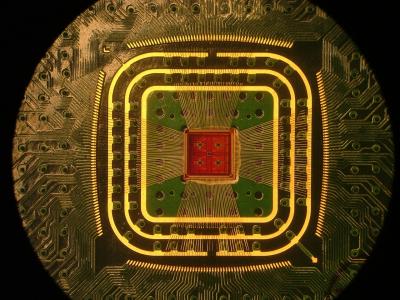 |
| This is a photograph of the Columbia Engineering team's custom multichannel CMOS preamplifier chip, attached to a circuit board with thin gold wirebonds.
Credit: Columbia Engineering |
Abstract:
As nanotechnology becomes ever more ubiquitous, researchers are using it to make medical diagnostics smaller, faster, and cheaper, in order to better diagnose diseases, learn more about inherited traits, and more. But as sensors get smaller, measuring them becomes more difficult—there is always a tradeoff between how long any measurement takes to make and how precise it is. And when a signal is very weak, the tradeoff is especially big.
Columbia Engineering and Penn researchers increase speed of single-molecule measurements: New integrated circuit design could lead to cheaper, faster DNA sequencing
New York, NY | Posted on March 18th, 2012A team of researchers at Columbia Engineering, led by Electrical Engineering Professor Ken Shepard, together with colleagues at the University of Pennsylvania, has figured out a way to measure nanopores—tiny holes in a thin membrane that can detect single biological molecules such as DNA and proteins—with less error than can be achieved with commercial instruments. They have miniaturized the measurement by designing a custom integrated circuit using commercial semiconductor technology, building the nanopore measurement around the new amplifier chip. Their research will be published in the Advance Online Publication on Nature Methods's website on 18 March at 1400 (2pm) US Eastern time/ 1800 London time.
Nanopores are exciting scientists because they may lead to extremely low-cost and fast DNA sequencing. But the signals from nanopores are very weak, so it is critically important to measure them as cleanly as possible.
"We put a tiny amplifier chip directly into the liquid chamber next to the nanopore, and the signals are so clean that we can see single molecules passing through the pore in only one microsecond," says Jacob Rosenstein, a Ph.D. candidate in electrical engineering at Columbia Engineering and lead author of the paper. "Previously, scientists could only see molecules that stay in the pore for more than 10 microseconds."
Many single-molecule measurements are currently made using optical techniques, which use fluorescent molecules that emit photons at a particular wavelength. But, while fluorescence is very powerful, its major limitation is that each molecule usually produces only a few thousand photons per second. "This means you can't see anything that happens faster than a few milliseconds, because any image you could take would be too dim," explains Shepard, who is Rosenstein's advisor. "On the other hand, if you can use techniques that measure electrons or ions, you can get billions of signals per second. The problem is that for electronic measurements there is no equivalent to a fluorescent wavelength filter, so even though the signal comes through, it is often buried in background noise."
Shepard's group has been interested in single-molecule measurements for several years looking at a variety of novel transduction platforms. They began working with nanopore sensors after Marija Drndic, a professor of physics at the University of Pennsylvania, gave a seminar at Columbia Engineering in 2009. "We saw that nearly everybody else measures nanopores using classical electrophysiology amplifiers, which are mostly optimized for slower measurements," notes Shepard. "So we designed our own integrated circuit instead."
Rosenstein designed the new electronics and did much of the lab work. Drndic's group at the University of Pennsylvania fabricated the nanopores that the team then measured in their new system.
"While most groups are trying to slow down DNA, our approach is to build faster electronics," says Drndic. "We combined the most sensitive electronics with the most sensitive solid-state nanopores."
"It's very exciting to be able to make purely electronic measurements of single molecules," says Rosenstein. "The setup for nanopore measurements is very simple and portable. It doesn't require a complicated microscope or high powered instruments; it just requires attention to detail. You can easily imagine nanopore technology having a major impact on DNA sequencing and other medical applications within the next few years."
Shepard's group is continuing to improve these techniques. "With a next-generation design," he says, "we may be able to get a further 10X improvement, and measure things that last only 100 nanoseconds. Our lab is also working with other electronic single-molecule techniques based on carbon nanotube transistors, which can leverage similar electronic circuits. This is an exciting time!"
This research has been funded by the National Institutes of Health, the Semiconductor Research Corporation, and the Office of Naval Research.
####
About Columbia University
Columbia University's Fu Foundation School of Engineering and Applied Science, founded in 1864, offers programs in nine departments to both undergraduate and graduate students. With facilities specifically designed and equipped to meet the laboratory and research needs of faculty and students, Columbia Engineering is home to NSF-NIH funded centers in genomic science, molecular nanostructures, materials science, and energy, as well as one of the world's leading programs in financial engineering. These interdisciplinary centers are leading the way in their respective fields while individual groups of engineers and scientists collaborate to solve some of modern society's more difficult challenges.
For more information, please click here
Contacts:
Holly Evarts
347-453-7408
Copyright © Columbia University
If you have a comment, please Contact us.Issuers of news releases, not 7th Wave, Inc. or Nanotechnology Now, are solely responsible for the accuracy of the content.
Bookmark:


| Related News Press |
News and information
![]() Simulating magnetization in a Heisenberg quantum spin chain April 5th, 2024
Simulating magnetization in a Heisenberg quantum spin chain April 5th, 2024
![]() NRL charters Navy’s quantum inertial navigation path to reduce drift April 5th, 2024
NRL charters Navy’s quantum inertial navigation path to reduce drift April 5th, 2024
![]() Discovery points path to flash-like memory for storing qubits: Rice find could hasten development of nonvolatile quantum memory April 5th, 2024
Discovery points path to flash-like memory for storing qubits: Rice find could hasten development of nonvolatile quantum memory April 5th, 2024
Govt.-Legislation/Regulation/Funding/Policy
![]() NRL charters Navy’s quantum inertial navigation path to reduce drift April 5th, 2024
NRL charters Navy’s quantum inertial navigation path to reduce drift April 5th, 2024
![]() Discovery points path to flash-like memory for storing qubits: Rice find could hasten development of nonvolatile quantum memory April 5th, 2024
Discovery points path to flash-like memory for storing qubits: Rice find could hasten development of nonvolatile quantum memory April 5th, 2024
![]() Chemical reactions can scramble quantum information as well as black holes April 5th, 2024
Chemical reactions can scramble quantum information as well as black holes April 5th, 2024
Chip Technology
![]() Discovery points path to flash-like memory for storing qubits: Rice find could hasten development of nonvolatile quantum memory April 5th, 2024
Discovery points path to flash-like memory for storing qubits: Rice find could hasten development of nonvolatile quantum memory April 5th, 2024
![]() Utilizing palladium for addressing contact issues of buried oxide thin film transistors April 5th, 2024
Utilizing palladium for addressing contact issues of buried oxide thin film transistors April 5th, 2024
![]() HKUST researchers develop new integration technique for efficient coupling of III-V and silicon February 16th, 2024
HKUST researchers develop new integration technique for efficient coupling of III-V and silicon February 16th, 2024
Nanomedicine
![]() New micromaterial releases nanoparticles that selectively destroy cancer cells April 5th, 2024
New micromaterial releases nanoparticles that selectively destroy cancer cells April 5th, 2024
![]() Good as gold - improving infectious disease testing with gold nanoparticles April 5th, 2024
Good as gold - improving infectious disease testing with gold nanoparticles April 5th, 2024
![]() Researchers develop artificial building blocks of life March 8th, 2024
Researchers develop artificial building blocks of life March 8th, 2024
Discoveries
![]() Chemical reactions can scramble quantum information as well as black holes April 5th, 2024
Chemical reactions can scramble quantum information as well as black holes April 5th, 2024
![]() New micromaterial releases nanoparticles that selectively destroy cancer cells April 5th, 2024
New micromaterial releases nanoparticles that selectively destroy cancer cells April 5th, 2024
![]() Utilizing palladium for addressing contact issues of buried oxide thin film transistors April 5th, 2024
Utilizing palladium for addressing contact issues of buried oxide thin film transistors April 5th, 2024
Announcements
![]() NRL charters Navy’s quantum inertial navigation path to reduce drift April 5th, 2024
NRL charters Navy’s quantum inertial navigation path to reduce drift April 5th, 2024
![]() Discovery points path to flash-like memory for storing qubits: Rice find could hasten development of nonvolatile quantum memory April 5th, 2024
Discovery points path to flash-like memory for storing qubits: Rice find could hasten development of nonvolatile quantum memory April 5th, 2024
Military
![]() NRL charters Navy’s quantum inertial navigation path to reduce drift April 5th, 2024
NRL charters Navy’s quantum inertial navigation path to reduce drift April 5th, 2024
![]() What heat can tell us about battery chemistry: using the Peltier effect to study lithium-ion cells March 8th, 2024
What heat can tell us about battery chemistry: using the Peltier effect to study lithium-ion cells March 8th, 2024
![]() New chip opens door to AI computing at light speed February 16th, 2024
New chip opens door to AI computing at light speed February 16th, 2024
|
|
||
|
|
||
| The latest news from around the world, FREE | ||
|
|
||
|
|
||
| Premium Products | ||
|
|
||
|
Only the news you want to read!
Learn More |
||
|
|
||
|
Full-service, expert consulting
Learn More |
||
|
|
||