Home > Press > Nano-imprinted photonic structures improve efficiency of silicon solar cells
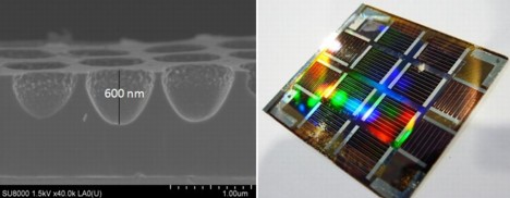 |
| nanoimprinted_solarcells.jpg: (left) Cross section SEM of the 2D periodic photonic nanostructures, (right) 1-�m-thin crystalline silicon solar cells on glass including the 2D periodic photonic nanostructures with obvious diffraction of light. |
Abstract:
Imec has successfully fabricated crystalline silicon (c-Si) solar cells including 2D periodic photonic nanostructures made with nano-imprint lithography. The result was an improvement in energy-conversion efficiency, compared to unpatterned cells, through a better absorption of the light spectrum. The technique shows a path to further reducing the thickness of solar cells while keeping the efficiency as high as possible.
Nano-imprinted photonic structures improve efficiency of silicon solar cells
Leuven, Belgium | Posted on March 16th, 2012The reduction of the silicon wafer thickness from 150μm to 50μm and below is potentially the best way to decrease the cost of solar cells. At imec, we pursue this path through ultrathin-film crystalline silicon technologies. However, if thinner photoactive layers are used, the optical absorption is significantly reduced. This is especially so at the near-infrared region of the solar spectrum. A photon with a wavelength of 1μm needs an absorption depth as deep as 100μm. Losing this part of the spectrum reduces the overall conversion efficiency of the cells.
Recently, the field of photonics has come up with methods to manipulate light through specific structures that are smaller than the wavelengths. This makes it possible to use periodic photonic nanostructures to affect the motion of photons in a similar way as the periodicity of atoms in a semiconductor crystal affects the motion of electrons. But to do so, we need efficient patterning techniques with nanometer-scale resolution.
At imec, we used nano-imprint lithography to fabricate 2D periodic photonic nanostructures. Nano-imprint lithography is a recent top-down approach for fabricating nanometer-scale patterns. It is one of the best candidates to improve the light absorption while maintaining an acceptable manufacturing cost, but it is currently barely used for c-Si PV applications. The patterning is performed by direct deformation of the resist material through mechanical pressure and a subsequent etching step.
Compared to the standard solar cell texturing by wet-etching, subwavelength patterning using nano-imprint lithography has some advantages. First, there is less material waste upon etching (less than a micron is consumed) compared to the state-of-the-art texturing, where 5-10 microns are lost. And second, diffraction and scattering of light is possible at higher angles due to the dimensions of the nanopattern.
####
For more information, please click here
Contacts:
Barbara Kalkis
Maestro Marketing & PR
Copyright © IMEC
If you have a comment, please Contact us.Issuers of news releases, not 7th Wave, Inc. or Nanotechnology Now, are solely responsible for the accuracy of the content.
Bookmark:


| Related News Press |
News and information
![]() Simulating magnetization in a Heisenberg quantum spin chain April 5th, 2024
Simulating magnetization in a Heisenberg quantum spin chain April 5th, 2024
![]() NRL charters Navy�s quantum inertial navigation path to reduce drift April 5th, 2024
NRL charters Navy�s quantum inertial navigation path to reduce drift April 5th, 2024
![]() Discovery points path to flash-like memory for storing qubits: Rice find could hasten development of nonvolatile quantum memory April 5th, 2024
Discovery points path to flash-like memory for storing qubits: Rice find could hasten development of nonvolatile quantum memory April 5th, 2024
Discoveries
![]() Chemical reactions can scramble quantum information as well as black holes April 5th, 2024
Chemical reactions can scramble quantum information as well as black holes April 5th, 2024
![]() New micromaterial releases nanoparticles that selectively destroy cancer cells April 5th, 2024
New micromaterial releases nanoparticles that selectively destroy cancer cells April 5th, 2024
![]() Utilizing palladium for addressing contact issues of buried oxide thin film transistors April 5th, 2024
Utilizing palladium for addressing contact issues of buried oxide thin film transistors April 5th, 2024
Announcements
![]() NRL charters Navy�s quantum inertial navigation path to reduce drift April 5th, 2024
NRL charters Navy�s quantum inertial navigation path to reduce drift April 5th, 2024
![]() Discovery points path to flash-like memory for storing qubits: Rice find could hasten development of nonvolatile quantum memory April 5th, 2024
Discovery points path to flash-like memory for storing qubits: Rice find could hasten development of nonvolatile quantum memory April 5th, 2024
Energy
![]() Development of zinc oxide nanopagoda array photoelectrode: photoelectrochemical water-splitting hydrogen production January 12th, 2024
Development of zinc oxide nanopagoda array photoelectrode: photoelectrochemical water-splitting hydrogen production January 12th, 2024
![]() Shedding light on unique conduction mechanisms in a new type of perovskite oxide November 17th, 2023
Shedding light on unique conduction mechanisms in a new type of perovskite oxide November 17th, 2023
![]() Inverted perovskite solar cell breaks 25% efficiency record: Researchers improve cell efficiency using a combination of molecules to address different November 17th, 2023
Inverted perovskite solar cell breaks 25% efficiency record: Researchers improve cell efficiency using a combination of molecules to address different November 17th, 2023
![]() The efficient perovskite cells with a structured anti-reflective layer � another step towards commercialization on a wider scale October 6th, 2023
The efficient perovskite cells with a structured anti-reflective layer � another step towards commercialization on a wider scale October 6th, 2023
Photonics/Optics/Lasers
![]() With VECSELs towards the quantum internet Fraunhofer: IAF achieves record output power with VECSEL for quantum frequency converters April 5th, 2024
With VECSELs towards the quantum internet Fraunhofer: IAF achieves record output power with VECSEL for quantum frequency converters April 5th, 2024
![]() Nanoscale CL thermometry with lanthanide-doped heavy-metal oxide in TEM March 8th, 2024
Nanoscale CL thermometry with lanthanide-doped heavy-metal oxide in TEM March 8th, 2024
![]() Optically trapped quantum droplets of light can bind together to form macroscopic complexes March 8th, 2024
Optically trapped quantum droplets of light can bind together to form macroscopic complexes March 8th, 2024
![]() HKUST researchers develop new integration technique for efficient coupling of III-V and silicon February 16th, 2024
HKUST researchers develop new integration technique for efficient coupling of III-V and silicon February 16th, 2024
Alliances/Trade associations/Partnerships/Distributorships
![]() Chicago Quantum Exchange welcomes six new partners highlighting quantum technology solutions, from Chicago and beyond September 23rd, 2022
Chicago Quantum Exchange welcomes six new partners highlighting quantum technology solutions, from Chicago and beyond September 23rd, 2022
![]() University of Illinois Chicago joins Brookhaven Lab's Quantum Center June 10th, 2022
University of Illinois Chicago joins Brookhaven Lab's Quantum Center June 10th, 2022
Solar/Photovoltaic
![]() Development of zinc oxide nanopagoda array photoelectrode: photoelectrochemical water-splitting hydrogen production January 12th, 2024
Development of zinc oxide nanopagoda array photoelectrode: photoelectrochemical water-splitting hydrogen production January 12th, 2024
![]() Shedding light on unique conduction mechanisms in a new type of perovskite oxide November 17th, 2023
Shedding light on unique conduction mechanisms in a new type of perovskite oxide November 17th, 2023
![]() Inverted perovskite solar cell breaks 25% efficiency record: Researchers improve cell efficiency using a combination of molecules to address different November 17th, 2023
Inverted perovskite solar cell breaks 25% efficiency record: Researchers improve cell efficiency using a combination of molecules to address different November 17th, 2023
![]() Charged �molecular beasts� the basis for new compounds: Researchers at Leipzig University use �aggressive� fragments of molecular ions for chemical synthesis November 3rd, 2023
Charged �molecular beasts� the basis for new compounds: Researchers at Leipzig University use �aggressive� fragments of molecular ions for chemical synthesis November 3rd, 2023
|
|
||
|
|
||
| The latest news from around the world, FREE | ||
|
|
||
|
|
||
| Premium Products | ||
|
|
||
|
Only the news you want to read!
Learn More |
||
|
|
||
|
Full-service, expert consulting
Learn More |
||
|
|
||