Home > Press > EU-funded BOOM project on SOI photonic integration technology successfully concluded
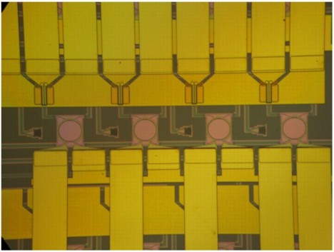 |
| BOOM: Four channel label extractor with four high-finesse ring resonators integrated with InGaAs photodetectors. |
Abstract:
Imec and its partners successfully completed ‘BOOM', a EU-funded project coordinated by the National Technical University of Athens (NTUA). By systematically advancing silicon-on-insulator (SOI) photonic integration technology, compact, cost-effective and power efficient components have been developed that enable photonic Tb/s capacity systems for current and new generation high-speed broadband core networks. As part of the project, imec has realized an optical label extractor consisting of a high-resolution demultiplexer integrated with highly efficient photodetectors.
EU-funded BOOM project on SOI photonic integration technology successfully concluded
Leuven, Belgium | Posted on March 15th, 2012The European BOOM project has focused on the development of a photonic routing platform relying on hybrid SOI integrated photonic ICs to implement all the routing functionalities: label detection (imec), control signal generation (HHI, IHP), wavelength conversion (NTUA, TU/e, TU Berlin) and wavelength routing (Lionix, AMO). Finally, a routing machine with >160Gb/s aggregate capacity (NTUA, Telecom Italia Lab) was built.
This way, the project answered the growing demand for bandwidth hungry internet applications which stresses the available capacity and performance of current optical core networks. Power efficiency, physical size and equipment cost are key issues in these networks and increasingly more difficult to keep within acceptable limits. Electronic carrier routing systems consume and dissipate large amounts of electrical power and heat respectively. By bringing photonics technologies deeper and deeper within these routers their performance can be improved and power consumption can be decreased.
The imec work within the project focused on the optical label detector. In the proposed routing architecture the optical data packets are labeled with a wavelength code, which has to be extracted from the packet and sent to the routing unit. The label extractor consists of an optical demultiplexer with very high resolution - 12.5GHz - fabricated on the imec silicon photonics platform and integrated with high efficiency photodetectors. Reaching the required resolution turned out to be very challenging and required an in depth study of silicon microring resonators. The required specifications could be reached using single ring resonator based filters. The ring resonators have integrated resistors, which allow fine tuning of the wavelength channels (bottom electrodes) through the thermo-optic effect. They are connected to evanescently coupled InGaAs photodetectors using the heterogeneous integration technology developed by INTEC, imec's associated laboratory at Ghent University. The detectors had an efficiency of close to 1A/W and were operating at the specified speed of 1GBit/s (up to 5GBit/s). Finally the device was packaged in collaboration with Fraunhofer IZM group (Berlin). The device is now ready for operation in a system test bed.
The results obtained by imec in the project and in particular the exhaustive study on the microring resonators are not only relevant for realizing the optical label extractor. They also form an important input for the imec optical interconnect program which requires high performance demultiplexers for increasing the bandwidth in optical chip-to-chip links. Further they can be used in optical sensors and non-linear devices.
####
For more information, please click here
Contacts:
Barbara Kalkis
Maestro Marketing & PR
Copyright © IMEC
If you have a comment, please Contact us.Issuers of news releases, not 7th Wave, Inc. or Nanotechnology Now, are solely responsible for the accuracy of the content.
Bookmark:


| Related News Press |
News and information
![]() Simulating magnetization in a Heisenberg quantum spin chain April 5th, 2024
Simulating magnetization in a Heisenberg quantum spin chain April 5th, 2024
![]() NRL charters Navy’s quantum inertial navigation path to reduce drift April 5th, 2024
NRL charters Navy’s quantum inertial navigation path to reduce drift April 5th, 2024
![]() Discovery points path to flash-like memory for storing qubits: Rice find could hasten development of nonvolatile quantum memory April 5th, 2024
Discovery points path to flash-like memory for storing qubits: Rice find could hasten development of nonvolatile quantum memory April 5th, 2024
Govt.-Legislation/Regulation/Funding/Policy
![]() NRL charters Navy’s quantum inertial navigation path to reduce drift April 5th, 2024
NRL charters Navy’s quantum inertial navigation path to reduce drift April 5th, 2024
![]() Discovery points path to flash-like memory for storing qubits: Rice find could hasten development of nonvolatile quantum memory April 5th, 2024
Discovery points path to flash-like memory for storing qubits: Rice find could hasten development of nonvolatile quantum memory April 5th, 2024
![]() Chemical reactions can scramble quantum information as well as black holes April 5th, 2024
Chemical reactions can scramble quantum information as well as black holes April 5th, 2024
Announcements
![]() NRL charters Navy’s quantum inertial navigation path to reduce drift April 5th, 2024
NRL charters Navy’s quantum inertial navigation path to reduce drift April 5th, 2024
![]() Discovery points path to flash-like memory for storing qubits: Rice find could hasten development of nonvolatile quantum memory April 5th, 2024
Discovery points path to flash-like memory for storing qubits: Rice find could hasten development of nonvolatile quantum memory April 5th, 2024
Photonics/Optics/Lasers
![]() With VECSELs towards the quantum internet Fraunhofer: IAF achieves record output power with VECSEL for quantum frequency converters April 5th, 2024
With VECSELs towards the quantum internet Fraunhofer: IAF achieves record output power with VECSEL for quantum frequency converters April 5th, 2024
![]() Nanoscale CL thermometry with lanthanide-doped heavy-metal oxide in TEM March 8th, 2024
Nanoscale CL thermometry with lanthanide-doped heavy-metal oxide in TEM March 8th, 2024
![]() Optically trapped quantum droplets of light can bind together to form macroscopic complexes March 8th, 2024
Optically trapped quantum droplets of light can bind together to form macroscopic complexes March 8th, 2024
![]() HKUST researchers develop new integration technique for efficient coupling of III-V and silicon February 16th, 2024
HKUST researchers develop new integration technique for efficient coupling of III-V and silicon February 16th, 2024
Alliances/Trade associations/Partnerships/Distributorships
![]() Chicago Quantum Exchange welcomes six new partners highlighting quantum technology solutions, from Chicago and beyond September 23rd, 2022
Chicago Quantum Exchange welcomes six new partners highlighting quantum technology solutions, from Chicago and beyond September 23rd, 2022
![]() University of Illinois Chicago joins Brookhaven Lab's Quantum Center June 10th, 2022
University of Illinois Chicago joins Brookhaven Lab's Quantum Center June 10th, 2022
|
|
||
|
|
||
| The latest news from around the world, FREE | ||
|
|
||
|
|
||
| Premium Products | ||
|
|
||
|
Only the news you want to read!
Learn More |
||
|
|
||
|
Full-service, expert consulting
Learn More |
||
|
|
||