Home > Press > Solved: The Mystery of the Nanoscale Crop Circles: In strange patterns of a gold-silicon alloy, Berkeley Lab scientists uncover unsuspected secrets and promising routes to nanoscale semiconductor processing
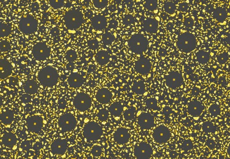 |
| When a thin layer of gold anneals on top of a silicon wafer coated with native silicon oxide, randomly distributed pools of eutectic alloy quickly form � and then go through a rapid series of strange changes, leaving behind bare silicon-dioxide circles surrounded by debris. Each denuded circle reveals a perfect square at its center. The area shown is about 107 by 155 micrometers (millionths of a meter). |
Abstract:
Almost three years ago a team of scientists at the U.S. Department of Energy's Lawrence Berkeley National Laboratory (Berkeley Lab) was performing an experiment in which layers of gold mere nanometers (billionths of a meter) thick were being heated on a flat silicon surface and then allowed to cool. They watched in surprise as peculiar features expanded and changed on the screen of their electron microscope, finally settling into circles surrounded by irregular blisters.
Solved: The Mystery of the Nanoscale Crop Circles: In strange patterns of a gold-silicon alloy, Berkeley Lab scientists uncover unsuspected secrets and promising routes to nanoscale semiconductor processing
Berkeley, CA | Posted on March 2nd, 2012The circles varied in diameter up to a few millionths of a meter, and in the center of each was a perfect square. The mysterious patterns were reminiscent of nothing so much as so‑called "alien" crop circles.
Until recently the cause of these strange formations remained a mystery. Now theoretical insights have explained what's happening, and the results have been published online by Physical Review Letters at prl.aps.org/abstract/PRL/v108/i9/e096102.
Eagerly melting alloys
When two solids are combined in just the right proportions, changes in chemical bonding may produce an alloy that melts at a temperature far lower than either can melt by itself. Such an alloy is called eutectic, Greek for "good melting." The eutectic alloy of gold and silicon - 81 percent gold and 19 percent silicon - is especially useful in processing nanoscale semiconductors such as nanowires, as well as for device interconnections in integrated circuits; it liquefies at a modest 363˚ Celsius, far lower than the melting point of either pure gold, 1064�C, or pure silicon, 1414�C.
"Gold-silicon eutectic liquid can safely solder chip layers together or form microscopic conducting wires, by flowing into channels in the substrate without burning up the surroundings," says Berkeley Lab's Junqiao Wu. "It's particularly interesting for processing nanoscale materials and devices." Wu cites the example of silicon nanowires, which can be grown from beads of eutectic liquid that form from droplets of gold. The beads catalyze the deposition of silicon from a chemical vapor and ride atop continually lengthening nanowire whiskers.
Understanding just how and why this happens has been a challenge. Although eutectic alloys are well studied as solids, the liquid state presents more obstacles, which are particularly formidable at the nanoscale because of greatly increased surface tension - the same surface forces that make it difficult to form ultra-thin films of water, for example, because they pull the water into droplets. At smaller scales the ratio of surface area to bulk increases markedly, and nanoscale structures have been described as virtually "all surface."
These are the conditions that the team led by Wu, who is a faculty scientist in Berkeley Lab's Materials Sciences Division and a professor in the Department of Materials Science and Engineering at the University of California at Berkeley, set out to examine, by creating the thinnest possible films of gold-silicon eutectic alloys. The researchers did so by starting with a substrate of pure silicon, on whose flat surface an extremely thin barrier layer (two nanometers thick) of silicon dioxide had formed. On this surface they laid layers of pure gold, varying the thickness from one trial to the next between just a few nanometers to a hefty 300 nanometers. The silicon dioxide barrier prevented the pure silicon from mixing with the gold.
The next step was to heat the layered sample to 600 �C for several minutes - not hot enough to melt the gold or silicon but hot enough to cause naturally existing pinholes in the thin silicon dioxide layer to enlarge into small weak spots, through which pure silicon could come in contact with the overlying gold. At the high temperature, silicon atoms quickly diffused out of the substrate and into the gold, forming a layer of eutectic gold-silicon alloy nearly the same thickness as the original gold and spreading in a virtually perfect circle from the central pinhole.
When the circular disk of eutectic alloy got large enough it suddenly broke up, disrupted by the high surface energy of the gold-silicon eutectic liquid. The debris was literally pulled to the edges of the disk, piling up around it to leave a central denuded zone of bare silicon dioxide.
In the center of the denuded zone, a perfect square of gold and silicon remained.
Chemistry and crystallography, not aliens
The researchers' most surprising discovery was that the thinner the original gold layer, the faster the eutectic circles expanded. The reaction rate when the gold layers were only 20 nanometers thick was more than 20 times faster than when the layers were 300 nanometers thick. And while at first glance the dimensions of the gold and silicon squares inside the circular denuded zones seemed variable, there was in fact a strict relation between the size of the square and the size of the circle: the radius of the circle was always the length of the square raised to the power of 3/2.
How did the squares get there in the first place? They originated as weak spots that were the sources of the spreading eutectic gold-silicon circles; when the circular eutectic was ruptured the squares filled with the same eutectic, which remained at the centers of the denuded zones. As they cooled, the gold and silicon within the squares separated, leaving sharply defined edges that were pure silicon; the centers were more roughly outlined squares of pure gold.
By slicing through the silicon/silicon dioxide/gold layercake and looking sideways at the structures with an electron microscope, the researchers found that the surface squares were the bases of inverted pyramids, resembling teeth penetrating the thin silicon dioxide layer and embedded in the silicon wafer. The squares were square, in fact, because of the silicon's orientation: the substrate had been cut along the crystal plane that defined the base. The four triangular sides of the pyramids lay along the low-energy planes of the crystal lattice and were defined by their intersections.
What began as a puzzling phenomenon reminiscent of "The X Files," if on a considerably smaller scale than the cosmic, the mystery of the "nanoscale crop circles" eventually yielded to careful observation and theoretical analysis - despite the obstacles posed by high temperatures, nanoscale sizes, instabilities of the liquid state, and extremely rapid time scales.
"We found that the reaction rate in forming small-sized gold-silicon eutectic liquids - and perhaps in many other eutectics as well - is dominated by the thickness of the reacting layers," says Wu. "This discovery may provide new routes for the engineering and processing of nanoscale materials."
####
About Berkeley Lab
DOE�s Office of Science is the single largest supporter of basic research in the physical sciences in the United States, and is working to address some of the most pressing challenges of our time. For more information, please visit science.energy.gov.
The Molecular Foundry is one of five DOE Nanoscale Science Research Centers (NSRCs), national user facilities for interdisciplinary research at the nanoscale, supported by the DOE Office of Science. Together the NSRCs comprise a suite of complementary facilities that provide researchers with state-of-the-art capabilities to fabricate, process, characterize, and model nanoscale materials, and constitute the largest infrastructure investment of the National Nanotechnology Initiative. The NSRCs are located at DOE�s Argonne, Brookhaven, Lawrence Berkeley, Oak Ridge and Sandia, and Los Alamos National Laboratories. For more information about the DOE NSRCs, please visit science.energy.gov.
Lawrence Berkeley National Laboratory addresses the world�s most urgent scientific challenges by advancing sustainable energy, protecting human health, creating new materials, and revealing the origin and fate of the universe. Founded in 1931, Berkeley Lab�s scientific expertise has been recognized with 13 Nobel prizes. The University of California manages Berkeley Lab for the U.S. Department of Energy�s Office of Science. For more, visit www.lbl.gov.
For more information, please click here
Contacts:
Paul Preuss
510-486-6249
Copyright © Berkeley Lab
If you have a comment, please Contact us.Issuers of news releases, not 7th Wave, Inc. or Nanotechnology Now, are solely responsible for the accuracy of the content.
Bookmark:


| Related Links |
![]() High-resolution details are at:
High-resolution details are at:
| Related News Press |
News and information
![]() Simulating magnetization in a Heisenberg quantum spin chain April 5th, 2024
Simulating magnetization in a Heisenberg quantum spin chain April 5th, 2024
![]() NRL charters Navy�s quantum inertial navigation path to reduce drift April 5th, 2024
NRL charters Navy�s quantum inertial navigation path to reduce drift April 5th, 2024
![]() Discovery points path to flash-like memory for storing qubits: Rice find could hasten development of nonvolatile quantum memory April 5th, 2024
Discovery points path to flash-like memory for storing qubits: Rice find could hasten development of nonvolatile quantum memory April 5th, 2024
Chemistry
![]() What heat can tell us about battery chemistry: using the Peltier effect to study lithium-ion cells March 8th, 2024
What heat can tell us about battery chemistry: using the Peltier effect to study lithium-ion cells March 8th, 2024
![]() Nanoscale CL thermometry with lanthanide-doped heavy-metal oxide in TEM March 8th, 2024
Nanoscale CL thermometry with lanthanide-doped heavy-metal oxide in TEM March 8th, 2024
![]() Focused ion beam technology: A single tool for a wide range of applications January 12th, 2024
Focused ion beam technology: A single tool for a wide range of applications January 12th, 2024
Laboratories
![]() A battery�s hopping ions remember where they�ve been: Seen in atomic detail, the seemingly smooth flow of ions through a battery�s electrolyte is surprisingly complicated February 16th, 2024
A battery�s hopping ions remember where they�ve been: Seen in atomic detail, the seemingly smooth flow of ions through a battery�s electrolyte is surprisingly complicated February 16th, 2024
![]() NRL discovers two-dimensional waveguides February 16th, 2024
NRL discovers two-dimensional waveguides February 16th, 2024
Videos/Movies
![]() New X-ray imaging technique to study the transient phases of quantum materials December 29th, 2022
New X-ray imaging technique to study the transient phases of quantum materials December 29th, 2022
![]() Solvent study solves solar cell durability puzzle: Rice-led project could make perovskite cells ready for prime time September 23rd, 2022
Solvent study solves solar cell durability puzzle: Rice-led project could make perovskite cells ready for prime time September 23rd, 2022
![]() Scientists prepare for the world�s smallest race: Nanocar Race II March 18th, 2022
Scientists prepare for the world�s smallest race: Nanocar Race II March 18th, 2022
![]() Visualizing the invisible: New fluorescent DNA label reveals nanoscopic cancer features March 4th, 2022
Visualizing the invisible: New fluorescent DNA label reveals nanoscopic cancer features March 4th, 2022
Govt.-Legislation/Regulation/Funding/Policy
![]() NRL charters Navy�s quantum inertial navigation path to reduce drift April 5th, 2024
NRL charters Navy�s quantum inertial navigation path to reduce drift April 5th, 2024
![]() Discovery points path to flash-like memory for storing qubits: Rice find could hasten development of nonvolatile quantum memory April 5th, 2024
Discovery points path to flash-like memory for storing qubits: Rice find could hasten development of nonvolatile quantum memory April 5th, 2024
![]() Chemical reactions can scramble quantum information as well as black holes April 5th, 2024
Chemical reactions can scramble quantum information as well as black holes April 5th, 2024
Discoveries
![]() Chemical reactions can scramble quantum information as well as black holes April 5th, 2024
Chemical reactions can scramble quantum information as well as black holes April 5th, 2024
![]() New micromaterial releases nanoparticles that selectively destroy cancer cells April 5th, 2024
New micromaterial releases nanoparticles that selectively destroy cancer cells April 5th, 2024
![]() Utilizing palladium for addressing contact issues of buried oxide thin film transistors April 5th, 2024
Utilizing palladium for addressing contact issues of buried oxide thin film transistors April 5th, 2024
Announcements
![]() NRL charters Navy�s quantum inertial navigation path to reduce drift April 5th, 2024
NRL charters Navy�s quantum inertial navigation path to reduce drift April 5th, 2024
![]() Discovery points path to flash-like memory for storing qubits: Rice find could hasten development of nonvolatile quantum memory April 5th, 2024
Discovery points path to flash-like memory for storing qubits: Rice find could hasten development of nonvolatile quantum memory April 5th, 2024
|
|
||
|
|
||
| The latest news from around the world, FREE | ||
|
|
||
|
|
||
| Premium Products | ||
|
|
||
|
Only the news you want to read!
Learn More |
||
|
|
||
|
Full-service, expert consulting
Learn More |
||
|
|
||