Home > Press > ORNL microscopy reveals 'atomic antenna' behavior in graphene
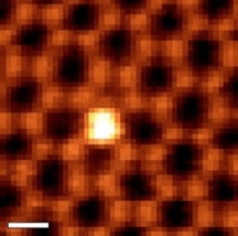 |
| Electron microscopy at Oak Ridge National Laboratory has demonstrated that silicon atoms (seen in white) can act like "atomic antennae" in graphene and transmit an electronic signal at the atomic scale. |
Abstract:
Atomic-level defects in graphene could be a path forward to smaller and faster electronic devices, according to a study led by researchers at the Department of Energy's Oak Ridge National Laboratory.
ORNL microscopy reveals 'atomic antenna' behavior in graphene
Oak Ridge, TN | Posted on January 31st, 2012With unique properties and potential applications in areas from electronics to biodevices, graphene, which consists of a single sheet of carbon atoms, has been hailed as a rising star in the materials world. Now, an ORNL study published in Nature Nanotechnology suggests that point defects, composed of silicon atoms that replace individual carbon atoms in graphene, could aid attempts to transfer data on an atomic scale by coupling light with electrons.
"In this proof of concept experiment, we have shown that a tiny wire made up of a pair of single silicon atoms in graphene can be used to convert light into an electronic signal, transmit the signal and then convert the signal back into light," said coauthor Juan-Carlos Idrobo, who holds a joint appointment at ORNL and Vanderbilt University.
An ORNL-led team discovered this novel behavior by using aberration-corrected scanning transmission electron microscopy to image the plasmon response, or optical-like signals, of the point defects. The team's analysis found that the silicon atoms act like atomic-sized antennae, enhancing the local surface plasmon response of graphene, and creating a prototypical plasmonic device.
"The idea with plasmonic devices is that they can convert optical signals into electronic signals," Idrobo said. "So you could make really tiny wires, put light in one side of the wire, and that signal will be transformed into collective electron excitations known as plasmons. The plasmons will transmit the signal through the wire, come out the other side and be converted back to light."
Although other plasmonic devices have been demonstrated, previous research in surface plasmons has been focused primarily on metals, which has limited the scale at which the signal transfer occurs.
"When researchers use metal for plasmonic devices, they can usually only get down to 5 - 7 nanometers," said coauthor Wu Zhou. "But when you want to make things smaller, you always want to know the limit. Nobody thought we could get down to a single atom level."
In-depth analysis at the level of a single atom was made possible through the team's access to an electron microscope that is part of ORNL's Shared Research Equipment (ShaRE) User Facility.
"It is the one of only a few electron microscopes in the world that we can use to look at and study materials and obtain crystallography, chemistry, bonding, optical and plasmon properties at the atomic scale with single atom sensitivity and at low voltages," Idrobo said. "This is an ideal microscope for people who want to research carbon-based materials, such as graphene."
In addition to its microscopic observations, the ORNL team employed theoretical first-principles calculations to confirm the stability of the observed point defects. The full paper, titled "Atomically Localized Plasmon Enhancement in Monolayer Graphene," is available online here: www.nature.com/nnano/journal/vaop/ncurrent/full/nnano.2011.252.html.
Coauthors are ORNL's Jagjit Nanda; and Jaekwang Lee, Sokrates Pantelides and Stephen Pennycook, who are jointly affiliated with ORNL and Vanderbilt. The research was supported by DOE's Office of Science, which also sponsors ORNL's ShaRE User Facility; by the National Science Foundation; and by the McMinn Endowment at Vanderbilt University. The study used resources of the National Energy Research Scientific Computer Center, which is supported by DOE'S Office of Science.
####
About Oak Ridge National Laboratory
ORNL is managed by UT-Battelle for the Department of Energy's Office of Science. DOE's Office of Science is the single largest supporter of basic research in the physical sciences in the United States, and is working to address some of the most pressing challenges of our time. For more information, please visit science.energy.gov
For more information, please click here
Contacts:
Morgan McCorkle
Communications and Media Relations
865.574.7308
Copyright © Oak Ridge National Laboratory
If you have a comment, please Contact us.Issuers of news releases, not 7th Wave, Inc. or Nanotechnology Now, are solely responsible for the accuracy of the content.
Bookmark:


| Related News Press |
News and information
![]() Simulating magnetization in a Heisenberg quantum spin chain April 5th, 2024
Simulating magnetization in a Heisenberg quantum spin chain April 5th, 2024
![]() NRL charters Navy�s quantum inertial navigation path to reduce drift April 5th, 2024
NRL charters Navy�s quantum inertial navigation path to reduce drift April 5th, 2024
![]() Discovery points path to flash-like memory for storing qubits: Rice find could hasten development of nonvolatile quantum memory April 5th, 2024
Discovery points path to flash-like memory for storing qubits: Rice find could hasten development of nonvolatile quantum memory April 5th, 2024
Graphene/ Graphite
![]() NRL discovers two-dimensional waveguides February 16th, 2024
NRL discovers two-dimensional waveguides February 16th, 2024
Laboratories
![]() A battery�s hopping ions remember where they�ve been: Seen in atomic detail, the seemingly smooth flow of ions through a battery�s electrolyte is surprisingly complicated February 16th, 2024
A battery�s hopping ions remember where they�ve been: Seen in atomic detail, the seemingly smooth flow of ions through a battery�s electrolyte is surprisingly complicated February 16th, 2024
![]() NRL discovers two-dimensional waveguides February 16th, 2024
NRL discovers two-dimensional waveguides February 16th, 2024
Govt.-Legislation/Regulation/Funding/Policy
![]() NRL charters Navy�s quantum inertial navigation path to reduce drift April 5th, 2024
NRL charters Navy�s quantum inertial navigation path to reduce drift April 5th, 2024
![]() Discovery points path to flash-like memory for storing qubits: Rice find could hasten development of nonvolatile quantum memory April 5th, 2024
Discovery points path to flash-like memory for storing qubits: Rice find could hasten development of nonvolatile quantum memory April 5th, 2024
![]() Chemical reactions can scramble quantum information as well as black holes April 5th, 2024
Chemical reactions can scramble quantum information as well as black holes April 5th, 2024
Discoveries
![]() Chemical reactions can scramble quantum information as well as black holes April 5th, 2024
Chemical reactions can scramble quantum information as well as black holes April 5th, 2024
![]() New micromaterial releases nanoparticles that selectively destroy cancer cells April 5th, 2024
New micromaterial releases nanoparticles that selectively destroy cancer cells April 5th, 2024
![]() Utilizing palladium for addressing contact issues of buried oxide thin film transistors April 5th, 2024
Utilizing palladium for addressing contact issues of buried oxide thin film transistors April 5th, 2024
Announcements
![]() NRL charters Navy�s quantum inertial navigation path to reduce drift April 5th, 2024
NRL charters Navy�s quantum inertial navigation path to reduce drift April 5th, 2024
![]() Discovery points path to flash-like memory for storing qubits: Rice find could hasten development of nonvolatile quantum memory April 5th, 2024
Discovery points path to flash-like memory for storing qubits: Rice find could hasten development of nonvolatile quantum memory April 5th, 2024
|
|
||
|
|
||
| The latest news from around the world, FREE | ||
|
|
||
|
|
||
| Premium Products | ||
|
|
||
|
Only the news you want to read!
Learn More |
||
|
|
||
|
Full-service, expert consulting
Learn More |
||
|
|
||