Home > Press > Down to the wire for silicon: Researchers create a wire 4 atoms wide, 1 atom tall
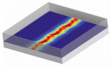 |
| Wires just one atom tall have been created by inserting a string of phosphorus atoms in a silicon crystal by a team of researchers from the Univeristy of New South Wales, Melbourne Univeristy and Purdue University. This image from a computational simulation run of the wires shows electron density as electrons flow from left to right. The wires are 20 times smaller than the smallest wires now available and measure just four atoms wide by one phosphorus atom tall. (Purdue University image/Sunhee Lee, Hoon Ryu and Gerhard Klimeck) |
Abstract:
Ohm's Law Survives to the Atomic Scale
B. Weber; S. Mahapatra; A. Fuhrer; T.C.G. Reusch; D. L. Thompson; W.C.T. Lee;
M.Y. Simmons, University of South Wales
H. Ryu; S. Lee; G. Klimeck, Purdue University
L.C.L. Hollenberg, Univeristy of Melbourne
A. Fuhrer, IBM Research-Zurich
As silicon electronics approaches the atomic scale, interconnects and circuitry become comparable in size to the active device components. Maintaining low electrical resistivity at this scale is challenging because of the presence of confining surfaces and interfaces. We report on the fabircation of wires in silicon—only one atom tall and four atoms wide—with exceptionally low resistivity (~0.3 milliohm-centimeters) and the current-carrying capabilities of copper. By embedding phosphorus atoms within a silicon crystal with an average spacing of less than one nanometer, we achieved a diameter-independent resitivity, which demonstrates Ohmic scaling to the atomic limit. Atomistic tight-binding calculations confirm the metallicity of these atomic-scale wires, which pave the way for single-atom device architecture for both classical and quantum information processing.
Down to the wire for silicon: Researchers create a wire 4 atoms wide, 1 atom tall
West Lafayette, IN | Posted on January 5th, 2012The smallest wires ever developed in silicon - just one atom tall and four atoms wide - have been shown by a team of researchers from the University of New South Wales, Melbourne University and Purdue University to have the same current-carrying capability as copper wires.
Experiments and atom-by-atom supercomputer models of the wires have found that the wires maintain a low capacity for resistance despite being more than 20 times thinner than conventional copper wires in microprocessors.
The discovery, which was published in this week's journal Science, has several implications, including:
* For engineers it could provide a roadmap to future nanoscale computational devices where atomic sizes are at the end of Moore's law. The theory shows that a single dense row of phosphorus atoms embedded in silicon will be the ultimate limit of downscaling.
* For computer scientists, it places donor-atom based silicon quantum computing closer to realization.
* And for physicists, the results show that Ohm's Law, which demonstrates the relationship between electrical current, resistance and voltage, continues to apply all the way down to an atomic-scale wire.
Bent Weber, the paper's lead author and a graduate student in the Centre of Excellence for Quantum Computation and Communication Technology at the University of New South Wales, was thrilled with the finding.
"It's extraordinary to show that Ohm's Law, such a basic law, still holds even when constructing a wire from the fundamental building blocks of nature - atoms," he says.
The innovation of the Australian group was to build the circuits up atom by atom, instead of the current method of building microprocessors, in which material is stripped away, says Gerhard Klimeck, a Purdue professor of electrical and computer engineering and director of the Network for Computational Nanotechnology.
"Typically we chip or etch material away, which can be very expensive, difficult and inaccurate," Klimeck says. "Once you get to 20 atoms wide you have atomic flucuations that make scaling difficult. But this experimental group built devices by placing atomically thin layers of phosphorus in silicon and found that with densely doped phosphorus wires just four atoms wide it acts like a wire that conducts just as well as metal."
The goal of the research is to develop future quantum computers in which single atoms are used for the computation, says Michelle Simmons, director of the Centre of Excellence for Quantum Computation and Communication Technology at the University of New South Wales and the project's principal investigator.
"We are on the threshold of making transistors out of individual atoms," Simmons says. "But to build a practical quantum computer we have recognized that the interconnecting wiring and circuitry also needs to shrink to the atomic scale."
Hoon Ryu, a Purdue graduate who is now a senior researcher with the Korea Institute of Science and Technology's Supercomputing Center, said the practicality of the research is exciting.
"The metallic wire is in principle quite difficult to be scaled into one- to two-nanometer pitch, but in both experimental and modeling views, the research result is quite remarkable," Ryu says. "For the first time, this demonstrates the possibility that densely doping wire is a viable alternative for the next-gerenation, ultra-scale metallic interconnect in silicon chips."
To assist the Australian researchers, Klimeck's research team ran hundreds of simulations to study the variability of these nanoscale structures.
"Having the throughput capability for a highly scalable code is important for doing that, and we have that capability here at Purdue with http://nanoHUB.org," Klimeck says. "We ran hundreds of cases to understand the potential landscape of these devices, so this was computationally intensive work."
Klimeck says that in addition to the project's scientific and engineering implications, he found the collaboration the most rewarding aspect.
"It is an exciting collaboration," he says. "We were doing simulations of experimental work, which was based on a theoretical model. So we were bringing the three legs of modern science together in one project. Plus, our graduate students are able to stay in contact and work with each other despite working in various locations around the world. It's hard to think of a better example of how science is done today."
####
For more information, please click here
Contacts:
Writer:
Steve Tally
765-494-9809
Twitter: sciencewriter
Media contacts:
Greg Kline
765-494-8167
University of New South Wales
media contact:
Mary O’Malley
0438 881 124
Sources:
Michelle Simmons
0425 336 756
Gerhard Klimeck
765-494-9212
Hoon Ryu
Copyright © Purdue University
If you have a comment, please Contact us.Issuers of news releases, not 7th Wave, Inc. or Nanotechnology Now, are solely responsible for the accuracy of the content.
Bookmark:


| Related News Press |
Physics
![]() Simulating magnetization in a Heisenberg quantum spin chain April 5th, 2024
Simulating magnetization in a Heisenberg quantum spin chain April 5th, 2024
News and information
![]() Simulating magnetization in a Heisenberg quantum spin chain April 5th, 2024
Simulating magnetization in a Heisenberg quantum spin chain April 5th, 2024
![]() NRL charters Navy’s quantum inertial navigation path to reduce drift April 5th, 2024
NRL charters Navy’s quantum inertial navigation path to reduce drift April 5th, 2024
![]() Discovery points path to flash-like memory for storing qubits: Rice find could hasten development of nonvolatile quantum memory April 5th, 2024
Discovery points path to flash-like memory for storing qubits: Rice find could hasten development of nonvolatile quantum memory April 5th, 2024
Quantum Computing
![]() Simulating magnetization in a Heisenberg quantum spin chain April 5th, 2024
Simulating magnetization in a Heisenberg quantum spin chain April 5th, 2024
![]() Discovery points path to flash-like memory for storing qubits: Rice find could hasten development of nonvolatile quantum memory April 5th, 2024
Discovery points path to flash-like memory for storing qubits: Rice find could hasten development of nonvolatile quantum memory April 5th, 2024
![]() With VECSELs towards the quantum internet Fraunhofer: IAF achieves record output power with VECSEL for quantum frequency converters April 5th, 2024
With VECSELs towards the quantum internet Fraunhofer: IAF achieves record output power with VECSEL for quantum frequency converters April 5th, 2024
![]() Chemical reactions can scramble quantum information as well as black holes April 5th, 2024
Chemical reactions can scramble quantum information as well as black holes April 5th, 2024
Discoveries
![]() Chemical reactions can scramble quantum information as well as black holes April 5th, 2024
Chemical reactions can scramble quantum information as well as black holes April 5th, 2024
![]() New micromaterial releases nanoparticles that selectively destroy cancer cells April 5th, 2024
New micromaterial releases nanoparticles that selectively destroy cancer cells April 5th, 2024
![]() Utilizing palladium for addressing contact issues of buried oxide thin film transistors April 5th, 2024
Utilizing palladium for addressing contact issues of buried oxide thin film transistors April 5th, 2024
Announcements
![]() NRL charters Navy’s quantum inertial navigation path to reduce drift April 5th, 2024
NRL charters Navy’s quantum inertial navigation path to reduce drift April 5th, 2024
![]() Discovery points path to flash-like memory for storing qubits: Rice find could hasten development of nonvolatile quantum memory April 5th, 2024
Discovery points path to flash-like memory for storing qubits: Rice find could hasten development of nonvolatile quantum memory April 5th, 2024
Research partnerships
![]() Discovery points path to flash-like memory for storing qubits: Rice find could hasten development of nonvolatile quantum memory April 5th, 2024
Discovery points path to flash-like memory for storing qubits: Rice find could hasten development of nonvolatile quantum memory April 5th, 2024
![]() Researchers’ approach may protect quantum computers from attacks March 8th, 2024
Researchers’ approach may protect quantum computers from attacks March 8th, 2024
![]() 'Sudden death' of quantum fluctuations defies current theories of superconductivity: Study challenges the conventional wisdom of superconducting quantum transitions January 12th, 2024
'Sudden death' of quantum fluctuations defies current theories of superconductivity: Study challenges the conventional wisdom of superconducting quantum transitions January 12th, 2024
Quantum nanoscience
![]() Simulating magnetization in a Heisenberg quantum spin chain April 5th, 2024
Simulating magnetization in a Heisenberg quantum spin chain April 5th, 2024
![]() Optically trapped quantum droplets of light can bind together to form macroscopic complexes March 8th, 2024
Optically trapped quantum droplets of light can bind together to form macroscopic complexes March 8th, 2024
![]() Bridging light and electrons January 12th, 2024
Bridging light and electrons January 12th, 2024
![]() 'Sudden death' of quantum fluctuations defies current theories of superconductivity: Study challenges the conventional wisdom of superconducting quantum transitions January 12th, 2024
'Sudden death' of quantum fluctuations defies current theories of superconductivity: Study challenges the conventional wisdom of superconducting quantum transitions January 12th, 2024
|
|
||
|
|
||
| The latest news from around the world, FREE | ||
|
|
||
|
|
||
| Premium Products | ||
|
|
||
|
Only the news you want to read!
Learn More |
||
|
|
||
|
Full-service, expert consulting
Learn More |
||
|
|
||