Home > Press > “Nanowiggles:” Scientists Discover Graphene Nanomaterials With Tunable Functionality in Electronics: Nanowiggles Can Be Customized To Produce Specific Band Gap and Magnetic Properties
 |
Abstract:
Electronics are getting smaller and smaller, flirting with new devices at the atomic scale. However, many scientists predict that the shrinking of our technology is reaching an end. Without an alternative to silicon-based technologies, the miniaturization of our electronics will stop. One promising alternative is graphene — the thinnest material known to man. Pure graphene is not a semiconductor, but it can be altered to display exceptional electrical behavior. Finding the best graphene-based nanomaterials could usher in a new era of nanoelectronics, optics, and spintronics (an emerging technology that uses the spin of electrons to store and process information in exceptionally small electronics).
“Nanowiggles:” Scientists Discover Graphene Nanomaterials With Tunable Functionality in Electronics: Nanowiggles Can Be Customized To Produce Specific Band Gap and Magnetic Properties
Troy, NY | Posted on January 4th, 2012Scientists at Rensselaer Polytechnic Institute have used the capabilities of one of the world's most powerful university-based supercomputers, the Rensselaer Center for Nanotechnology Innovations (CCNI), to uncover the properties of a promising form of graphene, known as graphene nanowiggles. What they found was that graphitic nanoribbons can be segmented into several different surface structures called nanowiggles. Each of these structures produces highly different magnetic and conductive properties. The findings provide a blueprint that scientists can use to literally pick and choose a graphene nanostructure that is tuned and customized for a different task or device. The work provides an important base of knowledge on these highly useful nanomaterials.
The findings were published in the journal Physical Review Letters in a paper titled "Emergence of Atypical Properties in Assembled Graphene Nanoribbons."
"Graphene nanomaterials have plenty of nice properties, but to date it has been very difficult to build defect-free graphene nanostructures. So these hard-to-reproduce nanostructures created a near insurmountable barrier between innovation and the market," said Vincent Meunier, the Gail and Jeffrey L. Kodosky '70 Constellation Professor of Physics, Information Technology, and Entrepreneurship at Rensselaer. "The advantage of graphene nanowiggles is that they can easily and quickly be produced very long and clean."
Nanowiggles were only recently discovered by a group led by scientists at EMPA, Switzerland. These particular nanoribbons are formed using a bottom-up approach, since they are chemically assembled atom by atom. This represents a very different approach to the standard graphene material design process that takes an existing material and attempts to cut it into a new structure. The process often creates a material that is not perfectly straight, but has small zigzags on its edges.
Meunier and his research team saw the potential of this new material. The nanowiggles could be easily manufactured and modified to display exceptional electrical conductive properties. Meunier and his team immediately set to work to dissect the nanowiggles to better understand possible future applications.
"What we found in our analysis of the nanowiggles' properties was even more surprising than previously thought," Meunier said.
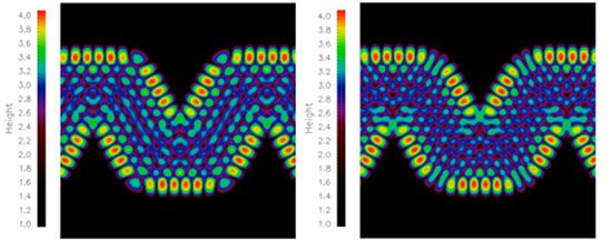
The scientists used computational analysis to study several different nanowiggle structures. The structures are named based on the shape of their edges and include armchair, armchair/zigzag, zigzag, and zigzag/armchair. All of the nanoribbon-edge structures have a wiggly appearance like a caterpillar inching across a leaf. Meunier named the four structures nanowiggles and each wiggle produced exceptionally different properties.
They found that the different nanowiggles produced highly varied band gaps. A band gap determines the levels of electrical conductivity of a solid material. They also found that different nanowiggles exhibited up to five highly varied magnetic properties. With this knowledge, scientists will be able to tune the bandgap and magnetic properties of a nanostructure based on their application, according to Meunier.
Meunier would like the research to inform the design of new and better devices. "We have created a roadmap that can allow for nanomaterials to be easily built and customized for applications from photovoltaics to semiconductors and, importantly, spintronics," he said.
By using CCNI, Meunier was able to complete these sophisticated calculations in a few months.
"Without CCNI, these calculations would still be continuing a year later and we would not yet have made this exciting discovery. Clearly this research is an excellent example illustrating the key role of CCNI in predictive fundamental science," he said.
####
For more information, please click here
Contacts:
Gabrielle DeMarco
Phone: (518) 276-6542
Copyright © Rensselaer Polytechnic Institute (RPI)
If you have a comment, please Contact us.Issuers of news releases, not 7th Wave, Inc. or Nanotechnology Now, are solely responsible for the accuracy of the content.
Bookmark:


| Related News Press |
News and information
![]() Simulating magnetization in a Heisenberg quantum spin chain April 5th, 2024
Simulating magnetization in a Heisenberg quantum spin chain April 5th, 2024
![]() NRL charters Navy’s quantum inertial navigation path to reduce drift April 5th, 2024
NRL charters Navy’s quantum inertial navigation path to reduce drift April 5th, 2024
![]() Discovery points path to flash-like memory for storing qubits: Rice find could hasten development of nonvolatile quantum memory April 5th, 2024
Discovery points path to flash-like memory for storing qubits: Rice find could hasten development of nonvolatile quantum memory April 5th, 2024
Graphene/ Graphite
![]() NRL discovers two-dimensional waveguides February 16th, 2024
NRL discovers two-dimensional waveguides February 16th, 2024
Spintronics
![]() Quantum materials: Electron spin measured for the first time June 9th, 2023
Quantum materials: Electron spin measured for the first time June 9th, 2023
![]() Linearly assembled Ag-Cu nanoclusters: Spin transfer and distance-dependent spin coupling November 4th, 2022
Linearly assembled Ag-Cu nanoclusters: Spin transfer and distance-dependent spin coupling November 4th, 2022
Chip Technology
![]() Discovery points path to flash-like memory for storing qubits: Rice find could hasten development of nonvolatile quantum memory April 5th, 2024
Discovery points path to flash-like memory for storing qubits: Rice find could hasten development of nonvolatile quantum memory April 5th, 2024
![]() Utilizing palladium for addressing contact issues of buried oxide thin film transistors April 5th, 2024
Utilizing palladium for addressing contact issues of buried oxide thin film transistors April 5th, 2024
![]() HKUST researchers develop new integration technique for efficient coupling of III-V and silicon February 16th, 2024
HKUST researchers develop new integration technique for efficient coupling of III-V and silicon February 16th, 2024
Nanoelectronics
![]() Interdisciplinary: Rice team tackles the future of semiconductors Multiferroics could be the key to ultralow-energy computing October 6th, 2023
Interdisciplinary: Rice team tackles the future of semiconductors Multiferroics could be the key to ultralow-energy computing October 6th, 2023
![]() Key element for a scalable quantum computer: Physicists from Forschungszentrum Jülich and RWTH Aachen University demonstrate electron transport on a quantum chip September 23rd, 2022
Key element for a scalable quantum computer: Physicists from Forschungszentrum Jülich and RWTH Aachen University demonstrate electron transport on a quantum chip September 23rd, 2022
![]() Reduced power consumption in semiconductor devices September 23rd, 2022
Reduced power consumption in semiconductor devices September 23rd, 2022
![]() Atomic level deposition to extend Moore’s law and beyond July 15th, 2022
Atomic level deposition to extend Moore’s law and beyond July 15th, 2022
Discoveries
![]() Chemical reactions can scramble quantum information as well as black holes April 5th, 2024
Chemical reactions can scramble quantum information as well as black holes April 5th, 2024
![]() New micromaterial releases nanoparticles that selectively destroy cancer cells April 5th, 2024
New micromaterial releases nanoparticles that selectively destroy cancer cells April 5th, 2024
![]() Utilizing palladium for addressing contact issues of buried oxide thin film transistors April 5th, 2024
Utilizing palladium for addressing contact issues of buried oxide thin film transistors April 5th, 2024
Announcements
![]() NRL charters Navy’s quantum inertial navigation path to reduce drift April 5th, 2024
NRL charters Navy’s quantum inertial navigation path to reduce drift April 5th, 2024
![]() Discovery points path to flash-like memory for storing qubits: Rice find could hasten development of nonvolatile quantum memory April 5th, 2024
Discovery points path to flash-like memory for storing qubits: Rice find could hasten development of nonvolatile quantum memory April 5th, 2024
Solar/Photovoltaic
![]() Development of zinc oxide nanopagoda array photoelectrode: photoelectrochemical water-splitting hydrogen production January 12th, 2024
Development of zinc oxide nanopagoda array photoelectrode: photoelectrochemical water-splitting hydrogen production January 12th, 2024
![]() Shedding light on unique conduction mechanisms in a new type of perovskite oxide November 17th, 2023
Shedding light on unique conduction mechanisms in a new type of perovskite oxide November 17th, 2023
![]() Inverted perovskite solar cell breaks 25% efficiency record: Researchers improve cell efficiency using a combination of molecules to address different November 17th, 2023
Inverted perovskite solar cell breaks 25% efficiency record: Researchers improve cell efficiency using a combination of molecules to address different November 17th, 2023
![]() Charged “molecular beasts” the basis for new compounds: Researchers at Leipzig University use “aggressive” fragments of molecular ions for chemical synthesis November 3rd, 2023
Charged “molecular beasts” the basis for new compounds: Researchers at Leipzig University use “aggressive” fragments of molecular ions for chemical synthesis November 3rd, 2023
|
|
||
|
|
||
| The latest news from around the world, FREE | ||
|
|
||
|
|
||
| Premium Products | ||
|
|
||
|
Only the news you want to read!
Learn More |
||
|
|
||
|
Full-service, expert consulting
Learn More |
||
|
|
||