Home > Press > New technique makes it easier to etch semiconductors
 |
| Graphic by Xiuling Li
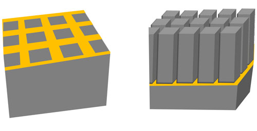
Metal-assisted chemical etching uses two steps. First, a thin layer of gold is patterned on top of a semiconductor wafer with soft lithography (left). The gold catalyzes a chemical reaction that etches the semiconductor form the top down, creating three-dimensional structures for optoelectronic applications (right). |
Abstract:
Creating semiconductor structures for high-end optoelectronic devices just got easier, thanks to University of Illinois researchers.
New technique makes it easier to etch semiconductors
Posted on December 22nd, 2011The team developed a method to chemically etch patterned arrays in the semiconductor gallium arsenide, used in solar cells, lasers, light emitting diodes (LEDs), field effect transistors (FETs), capacitors and sensors. Led by electrical and computer engineering professor Xiuling Li, the researchers describe their technique in the journal Nano Letters.
A semiconductor's physical properties can vary depending on its structure, so semiconductor wafers are etched into structures that tune their electrical and optical properties and connectivity before they are assembled into chips.
Semiconductors are commonly etched with two techniques: "Wet" etching uses a chemical solution to erode the semiconductor in all directions, while "dry" etching uses a directed beam of ions to bombard the surface, carving out a directed pattern. Such patterns are required for high-aspect-ratio nanostructures, or tiny shapes that have a large ratio of height to width. High-aspect-ratio structures are essential to many high-end optoelectronic device applications.
While silicon is the most ubiquitous material in semiconductor devices, materials in the III-V (pronounced three-five) group are more efficient in optoelectronic applications, such as solar cells or lasers.
Unfortunately, these materials can be difficult to dry etch, as the high-energy ion blasts damage the semiconductor's surface. III-V semiconductors are especially susceptible to damage.
To address this problem, Li and her group turned to metal-assisted chemical etching (MacEtch), a wet-etching approach they had previously developed for silicon. Unlike other wet methods, MacEtch works in one direction, from the top down. It is faster and less expensive than many dry etch techniques, according to Li. Her group revisited the MacEtch technique, optimizing the chemical solution and reaction conditions for the III-V semiconductor gallium arsenide (GaAs).
The process has two steps. First, a thin film of metal is patterned on the GaAs surface. Then, the semiconductor with the metal pattern is immersed in the MacEtch chemical solution. The metal catalyzes the reaction so that only the areas touching metal are etched away, and high-aspect-ratio structures are formed as the metal sinks into the wafer. When the etching is done, the metal can be cleaned from the surface without damaging it.
"It is a big deal to be able to etch GaAs this way," Li said. "The realization of high-aspect-ratio III-V nanostructure arrays by wet etching can potentially transform the fabrication of semiconductor lasers where surface grating is currently fabricated by dry etching, which is expensive and causes surface damage."
To create metal film patterns on the GaAs surface, Li's team used a patterning technique pioneered by John Rogers, the Lee J. Flory-Founder Chair and a professor of materials science and engineering at the U. of I. Their research teams joined forces to optimize the method, called soft lithography, for chemical compatibility while protecting the GaAs surface. Soft lithography is applied to the whole semiconductor wafer, as opposed to small segments, creating patterns over large areas - without expensive optical equipment.
"The combination of soft lithography and MacEtch make the perfect combination to produce large-area, high-aspect-ratio III-V nanostructures in a low-cost fashion," said Li, who is affiliated with the Micro and Nanotechnology Laboratory, the Frederick Seitz Materials Research Laboratory and the Beckman Institute for Advanced Science and Technology at the U. of I.
Next, the researchers hope to further optimize conditions for GaAs etching and establish parameters for MacEtch of other III-V semiconductors. Then, they hope to demonstrate device fabrication, including distributed Bragg reflector lasers and photonic crystals.
"MacEtch is a universal method as long as the right condition for deferential etching with and without metal can be found," Li said.
The Department of Energy and the National Science Foundation supported this work.
####
For more information, please click here
Contacts:
Liz Ahlberg
Physical Sciences Editor
217-244-1073
Xiuling Li
217-265-6354
Copyright © University of Illinois at Urbana-Champaign
If you have a comment, please Contact us.Issuers of news releases, not 7th Wave, Inc. or Nanotechnology Now, are solely responsible for the accuracy of the content.
Bookmark:


| Related Links |
| Related News Press |
News and information
![]() Simulating magnetization in a Heisenberg quantum spin chain April 5th, 2024
Simulating magnetization in a Heisenberg quantum spin chain April 5th, 2024
![]() NRL charters Navy�s quantum inertial navigation path to reduce drift April 5th, 2024
NRL charters Navy�s quantum inertial navigation path to reduce drift April 5th, 2024
![]() Discovery points path to flash-like memory for storing qubits: Rice find could hasten development of nonvolatile quantum memory April 5th, 2024
Discovery points path to flash-like memory for storing qubits: Rice find could hasten development of nonvolatile quantum memory April 5th, 2024
![]() Good as gold - improving infectious disease testing with gold nanoparticles April 5th, 2024
Good as gold - improving infectious disease testing with gold nanoparticles April 5th, 2024
Display technology/LEDs/SS Lighting/OLEDs
![]() Utilizing palladium for addressing contact issues of buried oxide thin film transistors April 5th, 2024
Utilizing palladium for addressing contact issues of buried oxide thin film transistors April 5th, 2024
![]() Light guide plate based on perovskite nanocomposites November 3rd, 2023
Light guide plate based on perovskite nanocomposites November 3rd, 2023
![]() Simple ballpoint pen can write custom LEDs August 11th, 2023
Simple ballpoint pen can write custom LEDs August 11th, 2023
Govt.-Legislation/Regulation/Funding/Policy
![]() NRL charters Navy�s quantum inertial navigation path to reduce drift April 5th, 2024
NRL charters Navy�s quantum inertial navigation path to reduce drift April 5th, 2024
![]() Discovery points path to flash-like memory for storing qubits: Rice find could hasten development of nonvolatile quantum memory April 5th, 2024
Discovery points path to flash-like memory for storing qubits: Rice find could hasten development of nonvolatile quantum memory April 5th, 2024
![]() Chemical reactions can scramble quantum information as well as black holes April 5th, 2024
Chemical reactions can scramble quantum information as well as black holes April 5th, 2024
Chip Technology
![]() Discovery points path to flash-like memory for storing qubits: Rice find could hasten development of nonvolatile quantum memory April 5th, 2024
Discovery points path to flash-like memory for storing qubits: Rice find could hasten development of nonvolatile quantum memory April 5th, 2024
![]() Utilizing palladium for addressing contact issues of buried oxide thin film transistors April 5th, 2024
Utilizing palladium for addressing contact issues of buried oxide thin film transistors April 5th, 2024
![]() HKUST researchers develop new integration technique for efficient coupling of III-V and silicon February 16th, 2024
HKUST researchers develop new integration technique for efficient coupling of III-V and silicon February 16th, 2024
Sensors
Nanoelectronics
![]() Interdisciplinary: Rice team tackles the future of semiconductors Multiferroics could be the key to ultralow-energy computing October 6th, 2023
Interdisciplinary: Rice team tackles the future of semiconductors Multiferroics could be the key to ultralow-energy computing October 6th, 2023
![]() Key element for a scalable quantum computer: Physicists from Forschungszentrum J�lich and RWTH Aachen University demonstrate electron transport on a quantum chip September 23rd, 2022
Key element for a scalable quantum computer: Physicists from Forschungszentrum J�lich and RWTH Aachen University demonstrate electron transport on a quantum chip September 23rd, 2022
![]() Reduced power consumption in semiconductor devices September 23rd, 2022
Reduced power consumption in semiconductor devices September 23rd, 2022
![]() Atomic level deposition to extend Moore�s law and beyond July 15th, 2022
Atomic level deposition to extend Moore�s law and beyond July 15th, 2022
Discoveries
![]() Chemical reactions can scramble quantum information as well as black holes April 5th, 2024
Chemical reactions can scramble quantum information as well as black holes April 5th, 2024
![]() New micromaterial releases nanoparticles that selectively destroy cancer cells April 5th, 2024
New micromaterial releases nanoparticles that selectively destroy cancer cells April 5th, 2024
![]() Utilizing palladium for addressing contact issues of buried oxide thin film transistors April 5th, 2024
Utilizing palladium for addressing contact issues of buried oxide thin film transistors April 5th, 2024
Announcements
![]() NRL charters Navy�s quantum inertial navigation path to reduce drift April 5th, 2024
NRL charters Navy�s quantum inertial navigation path to reduce drift April 5th, 2024
![]() Discovery points path to flash-like memory for storing qubits: Rice find could hasten development of nonvolatile quantum memory April 5th, 2024
Discovery points path to flash-like memory for storing qubits: Rice find could hasten development of nonvolatile quantum memory April 5th, 2024
Energy
![]() Development of zinc oxide nanopagoda array photoelectrode: photoelectrochemical water-splitting hydrogen production January 12th, 2024
Development of zinc oxide nanopagoda array photoelectrode: photoelectrochemical water-splitting hydrogen production January 12th, 2024
![]() Shedding light on unique conduction mechanisms in a new type of perovskite oxide November 17th, 2023
Shedding light on unique conduction mechanisms in a new type of perovskite oxide November 17th, 2023
![]() Inverted perovskite solar cell breaks 25% efficiency record: Researchers improve cell efficiency using a combination of molecules to address different November 17th, 2023
Inverted perovskite solar cell breaks 25% efficiency record: Researchers improve cell efficiency using a combination of molecules to address different November 17th, 2023
![]() The efficient perovskite cells with a structured anti-reflective layer � another step towards commercialization on a wider scale October 6th, 2023
The efficient perovskite cells with a structured anti-reflective layer � another step towards commercialization on a wider scale October 6th, 2023
Battery Technology/Capacitors/Generators/Piezoelectrics/Thermoelectrics/Energy storage
![]() What heat can tell us about battery chemistry: using the Peltier effect to study lithium-ion cells March 8th, 2024
What heat can tell us about battery chemistry: using the Peltier effect to study lithium-ion cells March 8th, 2024
![]() A battery�s hopping ions remember where they�ve been: Seen in atomic detail, the seemingly smooth flow of ions through a battery�s electrolyte is surprisingly complicated February 16th, 2024
A battery�s hopping ions remember where they�ve been: Seen in atomic detail, the seemingly smooth flow of ions through a battery�s electrolyte is surprisingly complicated February 16th, 2024
Solar/Photovoltaic
![]() Development of zinc oxide nanopagoda array photoelectrode: photoelectrochemical water-splitting hydrogen production January 12th, 2024
Development of zinc oxide nanopagoda array photoelectrode: photoelectrochemical water-splitting hydrogen production January 12th, 2024
![]() Shedding light on unique conduction mechanisms in a new type of perovskite oxide November 17th, 2023
Shedding light on unique conduction mechanisms in a new type of perovskite oxide November 17th, 2023
![]() Inverted perovskite solar cell breaks 25% efficiency record: Researchers improve cell efficiency using a combination of molecules to address different November 17th, 2023
Inverted perovskite solar cell breaks 25% efficiency record: Researchers improve cell efficiency using a combination of molecules to address different November 17th, 2023
![]() Charged �molecular beasts� the basis for new compounds: Researchers at Leipzig University use �aggressive� fragments of molecular ions for chemical synthesis November 3rd, 2023
Charged �molecular beasts� the basis for new compounds: Researchers at Leipzig University use �aggressive� fragments of molecular ions for chemical synthesis November 3rd, 2023
Printing/Lithography/Inkjet/Inks/Bio-printing/Dyes
![]() Presenting: Ultrasound-based printing of 3D materials�potentially inside the body December 8th, 2023
Presenting: Ultrasound-based printing of 3D materials�potentially inside the body December 8th, 2023
![]() Simple ballpoint pen can write custom LEDs August 11th, 2023
Simple ballpoint pen can write custom LEDs August 11th, 2023
![]() Disposable electronics on a simple sheet of paper October 7th, 2022
Disposable electronics on a simple sheet of paper October 7th, 2022
|
|
||
|
|
||
| The latest news from around the world, FREE | ||
|
|
||
|
|
||
| Premium Products | ||
|
|
||
|
Only the news you want to read!
Learn More |
||
|
|
||
|
Full-service, expert consulting
Learn More |
||
|
|
||