Home > Press > Instant nanodots grow on silicon to form sensing array: New methods for creating 3D nanostructures deposited on an array of regularly spaced indentations on the surface of silicon films opens the door for innovative nanosensors
 |
Abstract:
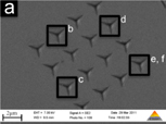
Scientists have shown that it is now possible to simultaneously create highly reproductive three-dimensional silicon oxide nanodots on micrometric scale silicon films in only a few seconds. Xavier Landreau and his colleagues at the University of Limoges, France, demonstrated in their paper to be published in EPJDą that they were able to create a square array of such nanodots, using regularly spaced nanoindents on the deposition layer, that could ultimately find applications as biosensors for genomics or bio-diagnostics.
Instant nanodots grow on silicon to form sensing array: New methods for creating 3D nanostructures deposited on an array of regularly spaced indentations on the surface of silicon films opens the door for innovative nanosensors
Heidelberg, Germany | Posted on December 2nd, 2011They used a process called atmospheric pressure plasma-enhanced chemical vapour deposition. This approach is a much faster alternative to methods such as nanoscale lithography, which only permits the deposition of one nanodot at a time. It also improves upon other silicon oxide growth processes that do not make it possible to precisely order the nanodots into an array. In addition, it can be carried out at atmospheric pressure, which decreases its costs compared to low-pressure deposition processes.
One of the authors' goals was to understand the self-organization mechanisms leading to a preferential deposition of the nanodots in the indents. By varying the indents' interspacing, they made it comparable to the average distance travelled by the silicon oxide particles of the deposited material. Thus, by adapting both the indents' spacing and the silicon substrate temperature, they observed optimum self-ordering inside the indents using atomic force microscopy.
The next step in their research will be to investigate how such nanoarrays could be used as nanosensors. They plan to develop similar square arrays on metallic substrates in order to better control the driving forces that produce the highly ordered self-organisation of nanodots. Further research will be needed to give sensing ability to individual nanodots by associating them with probe molecules designed to recognise target molecules to be detected.
Reference
1. Landreau X, Lanfant B, Merle T, Laborde E, Dublanche-Tixier C, Tristant P (2011). Ordering of SiOxHyCz islands deposited by atmospheric pressure microwave plasma torch on Si(100) substrates patterned by nanoindentation. European Physical Journal D (EPJ D). DOI 10.1140/epjd/e2011-20503-7
####
For more information, please click here
Contacts:
Corporate Communications Manager
Springer-Verlag
Tiergartenstrasse 17
69121 Heidelberg
Germany
Phone: +49 6221 487 81 30
Fax: +49 6221 487 68130
Copyright © Springer
If you have a comment, please Contact us.Issuers of news releases, not 7th Wave, Inc. or Nanotechnology Now, are solely responsible for the accuracy of the content.
Bookmark:


| Related Links |
| Related News Press |
News and information
![]() Simulating magnetization in a Heisenberg quantum spin chain April 5th, 2024
Simulating magnetization in a Heisenberg quantum spin chain April 5th, 2024
![]() NRL charters Navy’s quantum inertial navigation path to reduce drift April 5th, 2024
NRL charters Navy’s quantum inertial navigation path to reduce drift April 5th, 2024
![]() Discovery points path to flash-like memory for storing qubits: Rice find could hasten development of nonvolatile quantum memory April 5th, 2024
Discovery points path to flash-like memory for storing qubits: Rice find could hasten development of nonvolatile quantum memory April 5th, 2024
Nanomedicine
![]() New micromaterial releases nanoparticles that selectively destroy cancer cells April 5th, 2024
New micromaterial releases nanoparticles that selectively destroy cancer cells April 5th, 2024
![]() Good as gold - improving infectious disease testing with gold nanoparticles April 5th, 2024
Good as gold - improving infectious disease testing with gold nanoparticles April 5th, 2024
![]() Researchers develop artificial building blocks of life March 8th, 2024
Researchers develop artificial building blocks of life March 8th, 2024
Sensors
Discoveries
![]() Chemical reactions can scramble quantum information as well as black holes April 5th, 2024
Chemical reactions can scramble quantum information as well as black holes April 5th, 2024
![]() New micromaterial releases nanoparticles that selectively destroy cancer cells April 5th, 2024
New micromaterial releases nanoparticles that selectively destroy cancer cells April 5th, 2024
![]() Utilizing palladium for addressing contact issues of buried oxide thin film transistors April 5th, 2024
Utilizing palladium for addressing contact issues of buried oxide thin film transistors April 5th, 2024
Announcements
![]() NRL charters Navy’s quantum inertial navigation path to reduce drift April 5th, 2024
NRL charters Navy’s quantum inertial navigation path to reduce drift April 5th, 2024
![]() Discovery points path to flash-like memory for storing qubits: Rice find could hasten development of nonvolatile quantum memory April 5th, 2024
Discovery points path to flash-like memory for storing qubits: Rice find could hasten development of nonvolatile quantum memory April 5th, 2024
|
|
||
|
|
||
| The latest news from around the world, FREE | ||
|
|
||
|
|
||
| Premium Products | ||
|
|
||
|
Only the news you want to read!
Learn More |
||
|
|
||
|
Full-service, expert consulting
Learn More |
||
|
|
||