Home > Press > Interdigitated back-contact silicon solar cells above 23% efficiency
 |
Abstract:
Imec together with its silicon photovoltaic industrial affiliation program partners Schott Solar, Total, Photovoltech, GDF-SUEZ, Solland Solar, Kaneka and Dow Corning, have demonstrated an excellent conversion efficiency of 23.3% on interdigitated back-contact (IBC) silicon solar cells.
Interdigitated back-contact silicon solar cells above 23% efficiency
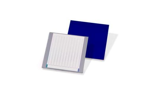
Leuven, Belgium | Posted on December 1st, 2011Interdigitated back contacts are introduced to increase the conversion efficiency of crystalline silicon solar cells and allow for further reduction of the cell thickness, simplification of module fabrication and improved aesthetics of the final solar cell modules. Imec has developed a high-efficiency baseline process for small-area IBC cells within its multi-partner silicon solar cells industrial affiliation program that aims at increasing the efficiency well above 20% and decreasing the cost of silicon solar cells beyond the current state-of-the-art.
Key aspects of the newly developed small-area (2x2 cm2) IBC Si solar cells are the n-type base float-zone (FZ) silicon substrates, a random pyramid texture, a boron diffused emitter, phosphorous diffused front- and back surface fields, a thermally grown silicon dioxide for surface passivation, a SiN single layer anti-reflective coating, lithography based patterning and Aluminum metallization. The realized IBC cells achieve a designated area conversion efficiency of 23.3% (Jsc = 41.6 mA, Voc=696 mV, FF=80.4%), certified by ISE-Callabs.
Jef Poortmans, director of imec's photovoltaic R&D program: "We are delighted to demonstrate these excellent efficiency results on IBC silicon solar cells. They prove the relevance of the IBC technology to our industrial partners. Such high efficiencies on small-area IBC silicon solar cells are a perfect base for further developing a large-area and industrially feasible IBC cell technology at imec."
"As silicon photovoltaic industrial affiliation program partners of imec we are very happy with this new result", says Dr. Martin Heming, CEO of SCHOTT Solar. This German solar manufacturer was the first industry partner to join imec's program on silicon solar cells. "The test result confirms our confidence in imec's excellent PV R&D capabilities and vision, and it allows us to acquire important know-how and IP as basis for our next generation solar cell products."
####
About IMEC
Imec performs world-leading research in nanoelectronics. Imec leverages its scientific knowledge with the innovative power of its global partnerships in ICT, healthcare and energy. Imec delivers industry-relevant technology solutions. In a unique high-tech environment, its international top talent is committed to providing the building blocks for a better life in a sustainable society. Imec is headquartered in Leuven, Belgium, and has offices in Belgium, the Netherlands, Taiwan, US, China, India and Japan. Its staff of about 1,900 people includes more than 500 industrial residents and guest researchers. In 2010, imec's revenue (P&L) was 285 million euro. Further information on imec can be found at www.imec.be.
Imec is a registered trademark for the activities of IMEC International (a legal entity set up under Belgian law as a "stichting van openbaar nut�), imec Belgium (IMEC vzw supported by the Flemish Government), imec the Netherlands (Stichting IMEC Nederland, part of Holst Centre which is supported by the Dutch Government), imec Taiwan (IMEC Taiwan Co.) and imec China (IMEC Microelectronics (Shangai) Co. Ltd.) and imec India (Imec India Private Limited).
For more information, please click here
Contacts:
Hanne Degans
External Communications Officer
T: +32 16 28 17 69
Mobile: +32 486 065 175
Barbara Kalkis
Maestro Marketing & PR
T : +1 408 996 9975
M : +1 408 529 4210
Copyright © IMEC
If you have a comment, please Contact us.Issuers of news releases, not 7th Wave, Inc. or Nanotechnology Now, are solely responsible for the accuracy of the content.
Bookmark:


| Related News Press |
News and information
![]() Simulating magnetization in a Heisenberg quantum spin chain April 5th, 2024
Simulating magnetization in a Heisenberg quantum spin chain April 5th, 2024
![]() NRL charters Navy�s quantum inertial navigation path to reduce drift April 5th, 2024
NRL charters Navy�s quantum inertial navigation path to reduce drift April 5th, 2024
![]() Discovery points path to flash-like memory for storing qubits: Rice find could hasten development of nonvolatile quantum memory April 5th, 2024
Discovery points path to flash-like memory for storing qubits: Rice find could hasten development of nonvolatile quantum memory April 5th, 2024
Announcements
![]() NRL charters Navy�s quantum inertial navigation path to reduce drift April 5th, 2024
NRL charters Navy�s quantum inertial navigation path to reduce drift April 5th, 2024
![]() Discovery points path to flash-like memory for storing qubits: Rice find could hasten development of nonvolatile quantum memory April 5th, 2024
Discovery points path to flash-like memory for storing qubits: Rice find could hasten development of nonvolatile quantum memory April 5th, 2024
Energy
![]() Development of zinc oxide nanopagoda array photoelectrode: photoelectrochemical water-splitting hydrogen production January 12th, 2024
Development of zinc oxide nanopagoda array photoelectrode: photoelectrochemical water-splitting hydrogen production January 12th, 2024
![]() Shedding light on unique conduction mechanisms in a new type of perovskite oxide November 17th, 2023
Shedding light on unique conduction mechanisms in a new type of perovskite oxide November 17th, 2023
![]() Inverted perovskite solar cell breaks 25% efficiency record: Researchers improve cell efficiency using a combination of molecules to address different November 17th, 2023
Inverted perovskite solar cell breaks 25% efficiency record: Researchers improve cell efficiency using a combination of molecules to address different November 17th, 2023
![]() The efficient perovskite cells with a structured anti-reflective layer � another step towards commercialization on a wider scale October 6th, 2023
The efficient perovskite cells with a structured anti-reflective layer � another step towards commercialization on a wider scale October 6th, 2023
Alliances/Trade associations/Partnerships/Distributorships
![]() Chicago Quantum Exchange welcomes six new partners highlighting quantum technology solutions, from Chicago and beyond September 23rd, 2022
Chicago Quantum Exchange welcomes six new partners highlighting quantum technology solutions, from Chicago and beyond September 23rd, 2022
![]() University of Illinois Chicago joins Brookhaven Lab's Quantum Center June 10th, 2022
University of Illinois Chicago joins Brookhaven Lab's Quantum Center June 10th, 2022
Solar/Photovoltaic
![]() Development of zinc oxide nanopagoda array photoelectrode: photoelectrochemical water-splitting hydrogen production January 12th, 2024
Development of zinc oxide nanopagoda array photoelectrode: photoelectrochemical water-splitting hydrogen production January 12th, 2024
![]() Shedding light on unique conduction mechanisms in a new type of perovskite oxide November 17th, 2023
Shedding light on unique conduction mechanisms in a new type of perovskite oxide November 17th, 2023
![]() Inverted perovskite solar cell breaks 25% efficiency record: Researchers improve cell efficiency using a combination of molecules to address different November 17th, 2023
Inverted perovskite solar cell breaks 25% efficiency record: Researchers improve cell efficiency using a combination of molecules to address different November 17th, 2023
![]() Charged �molecular beasts� the basis for new compounds: Researchers at Leipzig University use �aggressive� fragments of molecular ions for chemical synthesis November 3rd, 2023
Charged �molecular beasts� the basis for new compounds: Researchers at Leipzig University use �aggressive� fragments of molecular ions for chemical synthesis November 3rd, 2023
|
|
||
|
|
||
| The latest news from around the world, FREE | ||
|
|
||
|
|
||
| Premium Products | ||
|
|
||
|
Only the news you want to read!
Learn More |
||
|
|
||
|
Full-service, expert consulting
Learn More |
||
|
|
||