Home > Press > Graphene earns its stripes: New nanoscale electronic state discovered on graphene sheets
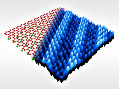 |
| These are electronic stripes, called "charge density waves," on the surface of a graphitic superconductor.
Credit: K. A. Rahnejat |
Abstract:
Researchers from the London Centre for Nanotechnology (LCN) have discovered electronic stripes, called 'charge density waves', on the surface of the graphene sheets that make up a graphitic superconductor. This is the first time these stripes have been seen on graphene, and the finding is likely to have profound implications for the exploitation of this recently discovered material, which scientists believe will play a key role in the future of nanotechnology. The discovery is reported in Nature Communications, 29th November.
Graphene earns its stripes: New nanoscale electronic state discovered on graphene sheets
London, UK | Posted on November 29th, 2011Graphene is a material made up of a single sheet of carbon atoms just one atom thick, and is found in the marks made by a graphite pencil. Graphene has remarkable physical properties and therefore has great technological potential, for example, in transparent electrodes for flat screen TVs, in fast energy-efficient transistors, and in ultra-strong composite materials. Scientists are now devoting huge efforts to understand and control the properties of this material.
The LCN team donated extra electrons to a graphene surface by sliding calcium metal atoms underneath it. One would normally expect these additional electrons to spread out evenly on the graphene surface, just as oil spreads out on water. But by using an instrument known as a scanning tunneling microscope, which can image individual atoms, the researchers have found that the extra electrons arrange themselves spontaneously into nanometer-scale stripes. This unexpected behavior demonstrates that the electrons can have a life of their own which is not connected directly to the underlying atoms. The results inspire many new directions for both science and technology. For example, they suggest a new method for manipulating and encoding information, where binary zeros and ones correspond to stripes running from north to south and running from east to west respectively.
This work is part of an ongoing multi-disciplinary research effort into graphene at the LCN and follows on from the original discovery of superconductivity in the graphite superconductor CaC6 by Weller at al. published in Nature Physics, doi:10.1038/nphys0010.
Professor Jan Zaanen of Leiden University and winner of the prestigious Spinoza prize for, among other things, his role as proponent of the stripe concept for atomically thin materials, commented: "This discovery is another important step towards demonstrating the ubiquity of stripes, and the fact that they appear in the world's simplest host - the two-dimensional network of carbon atoms that is graphene - means that more great science and applications are not far behind."
Notes to Editors:
The paper
'Charge density waves in the graphene sheets of the superconductor CaC6' appears in Nature Communications on 29th November 2001. DOI: 10.1038/ncomms1574
####
About University College London
The London Centre for Nanotechnology, is a UK-based, multidisciplinary research centre forming the bridge between the physical and biomedical sciences. It was conceived from the outset with a management structure allowing for a clear focus on scientific excellence, exploitation and commercialisation. It brings together two world leaders in nanotechnology, namely University College London and Imperial College London, in a unique operating model that accesses the combined skills of multiple departments, including medicine, chemistry, physics, electronic and electrical engineering, biochemical engineering, materials and earth sciences, and two leading technology transfer offices. Website: www.london-nano.com
For more information, please click here
Contacts:
Joanna Rooke
44-207-679-9950
Copyright © University College London
If you have a comment, please Contact us.Issuers of news releases, not 7th Wave, Inc. or Nanotechnology Now, are solely responsible for the accuracy of the content.
Bookmark:


| Related News Press |
News and information
![]() Simulating magnetization in a Heisenberg quantum spin chain April 5th, 2024
Simulating magnetization in a Heisenberg quantum spin chain April 5th, 2024
![]() NRL charters Navy�s quantum inertial navigation path to reduce drift April 5th, 2024
NRL charters Navy�s quantum inertial navigation path to reduce drift April 5th, 2024
![]() Discovery points path to flash-like memory for storing qubits: Rice find could hasten development of nonvolatile quantum memory April 5th, 2024
Discovery points path to flash-like memory for storing qubits: Rice find could hasten development of nonvolatile quantum memory April 5th, 2024
Graphene/ Graphite
![]() NRL discovers two-dimensional waveguides February 16th, 2024
NRL discovers two-dimensional waveguides February 16th, 2024
Chip Technology
![]() Discovery points path to flash-like memory for storing qubits: Rice find could hasten development of nonvolatile quantum memory April 5th, 2024
Discovery points path to flash-like memory for storing qubits: Rice find could hasten development of nonvolatile quantum memory April 5th, 2024
![]() Utilizing palladium for addressing contact issues of buried oxide thin film transistors April 5th, 2024
Utilizing palladium for addressing contact issues of buried oxide thin film transistors April 5th, 2024
![]() HKUST researchers develop new integration technique for efficient coupling of III-V and silicon February 16th, 2024
HKUST researchers develop new integration technique for efficient coupling of III-V and silicon February 16th, 2024
Memory Technology
![]() Utilizing palladium for addressing contact issues of buried oxide thin film transistors April 5th, 2024
Utilizing palladium for addressing contact issues of buried oxide thin film transistors April 5th, 2024
![]() Interdisciplinary: Rice team tackles the future of semiconductors Multiferroics could be the key to ultralow-energy computing October 6th, 2023
Interdisciplinary: Rice team tackles the future of semiconductors Multiferroics could be the key to ultralow-energy computing October 6th, 2023
![]() Researchers discover materials exhibiting huge magnetoresistance June 9th, 2023
Researchers discover materials exhibiting huge magnetoresistance June 9th, 2023
Discoveries
![]() Chemical reactions can scramble quantum information as well as black holes April 5th, 2024
Chemical reactions can scramble quantum information as well as black holes April 5th, 2024
![]() New micromaterial releases nanoparticles that selectively destroy cancer cells April 5th, 2024
New micromaterial releases nanoparticles that selectively destroy cancer cells April 5th, 2024
![]() Utilizing palladium for addressing contact issues of buried oxide thin film transistors April 5th, 2024
Utilizing palladium for addressing contact issues of buried oxide thin film transistors April 5th, 2024
Announcements
![]() NRL charters Navy�s quantum inertial navigation path to reduce drift April 5th, 2024
NRL charters Navy�s quantum inertial navigation path to reduce drift April 5th, 2024
![]() Discovery points path to flash-like memory for storing qubits: Rice find could hasten development of nonvolatile quantum memory April 5th, 2024
Discovery points path to flash-like memory for storing qubits: Rice find could hasten development of nonvolatile quantum memory April 5th, 2024
|
|
||
|
|
||
| The latest news from around the world, FREE | ||
|
|
||
|
|
||
| Premium Products | ||
|
|
||
|
Only the news you want to read!
Learn More |
||
|
|
||
|
Full-service, expert consulting
Learn More |
||
|
|
||