Home > Press > UCLA team develops highly efficient method for creating flexible, transparent electrodes
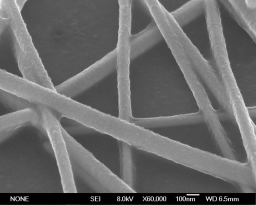 |
| Silver nanowire network |
Abstract:
As the market for liquid crystal displays and other electronics continues to drive up the price of indium — the material used to make the indium tin oxide (ITO) transparent electrodes in these devices — scientists have been searching for a less costly and more dynamic alternative, particularly for use in future flexible electronics.
UCLA team develops highly efficient method for creating flexible, transparent electrodes
Los Angeles, CA | Posted on November 22nd, 2011Besides its high price, ITO has several drawbacks. It's brittle, making it impractical for use in flexible displays and solar cells, and there is a lack of availability of indium, which is found primarily in Asia. Further, the production of ITO films is relatively inefficient.
Now, researchers at UCLA report in the journal ACS Nano that they have developed a unique method for producing transparent electrodes that uses silver nanowires in combination with other nanomaterials. The new electrodes are flexible and highly conductive and overcome the limitations associated with ITO.
For some time, silver nanowire (AgNW) networks have been seen as promising candidates to replace ITO because they are flexible and each wire is highly conductive. But complicated treatments have often been required to fuse crossed AgNWs to achieve low resistance and good substrate adhesion. To address this, the UCLA researchers demonstrated that by fusing AgNWs with metal-oxide nanoparticles and organic polymers, they could efficiently produce highly transparent conductors.
The team of researchers represents a collaboration between the department of materials science and engineering at the UCLA Henry Samueli School of Engineering and Applied Science; the department of chemistry and biochemistry in the UCLA College of Letters and Science; and the California NanoSystems Institute (CNSI) at UCLA.
The team was led by Yang Yang, a professor of materials science and engineering, and Paul Weiss, director of the CNSI and a professor of materials science and engineering and of chemistry and biochemistry.
"In this work, we demonstrate a simple and effective solution method to achieve highly conductive AgNW composite films with excellent optical transparency and mechanical properties," said Yang who also directs the Nano Renewable Energy Center at the CNSI. "This is by far the best solution: a processed, transparent electrode that is compatible with a wide variety of substrate choices."
Scientists can easily spray a surface with the nanowires to make a transparent mat, but the challenge is to make the silver nanowires adhere to the surface more securely without the use of extreme temperatures (200° C) or high pressures, steps that make the nanomaterials less compatible with the sensitive organic materials typically used to make flexible electronics.
To meet this challenge, Rui Zhu, the paper's first author, developed a low-temperature method to make high-performance transparent electrodes from silver nanowires using spray coating of a unique combination of nanomaterials.
First, researchers sprayed a solution of commercially available silver nanowires onto a surface. They then treated the nanowires with a solution of titanium dioxide nanoparticles to create a hybrid film. As the film dries, capillary forces pull the nanowires together, improving the film's conductivity. The scientists then coated the film with a layer of conductive polymer to increase the wires' adhesion to the surface.
The AgNW composite meshes are highly conductive, with excellent optical transparency and mechanical properties. The research team also built solar cells using the new electrodes and found that their performance was comparable to that of solar cells made with indium tin oxide.
The research received support from the Office of Naval Research and the Kavli Foundation.
####
About UCLA
The California NanoSystems Institute is an integrated research facility located at UCLA and UC Santa Barbara. Its mission is to foster interdisciplinary collaborations in nanoscience and nanotechnology; to train a new generation of scientists, educators and technology leaders; to generate partnerships with industry; and to contribute to the economic development and the social well-being of California, the United States and the world. The CNSI was established in 2000 with $100 million from the state of California. The total amount of research funding in nanoscience and nanotechnology awarded to CNSI members has risen to over $900 million. UCLA CNSI members are drawn from UCLA's College of Letters and Science, the David Geffen School of Medicine, the School of Dentistry, the School of Public Health and the Henry Samueli School of Engineering and Applied Science. They are engaged in measuring, modifying and manipulating atoms and molecules — the building blocks of our world. Their work is carried out in an integrated laboratory environment. This dynamic research setting has enhanced understanding of phenomena at the nanoscale and promises to produce important discoveries in health, energy, the environment and information technology.
For more information, please click here
Contacts:
Jennifer Marcus,
310-267-4839
Copyright © UCLA
If you have a comment, please Contact us.Issuers of news releases, not 7th Wave, Inc. or Nanotechnology Now, are solely responsible for the accuracy of the content.
Bookmark:


| Related News Press |
News and information
![]() Simulating magnetization in a Heisenberg quantum spin chain April 5th, 2024
Simulating magnetization in a Heisenberg quantum spin chain April 5th, 2024
![]() NRL charters Navy’s quantum inertial navigation path to reduce drift April 5th, 2024
NRL charters Navy’s quantum inertial navigation path to reduce drift April 5th, 2024
![]() Discovery points path to flash-like memory for storing qubits: Rice find could hasten development of nonvolatile quantum memory April 5th, 2024
Discovery points path to flash-like memory for storing qubits: Rice find could hasten development of nonvolatile quantum memory April 5th, 2024
![]() Good as gold - improving infectious disease testing with gold nanoparticles April 5th, 2024
Good as gold - improving infectious disease testing with gold nanoparticles April 5th, 2024
Display technology/LEDs/SS Lighting/OLEDs
![]() Utilizing palladium for addressing contact issues of buried oxide thin film transistors April 5th, 2024
Utilizing palladium for addressing contact issues of buried oxide thin film transistors April 5th, 2024
![]() Light guide plate based on perovskite nanocomposites November 3rd, 2023
Light guide plate based on perovskite nanocomposites November 3rd, 2023
![]() Simple ballpoint pen can write custom LEDs August 11th, 2023
Simple ballpoint pen can write custom LEDs August 11th, 2023
Flexible Electronics
![]() CityU awarded invention: Soft, ultrathin photonic material cools down wearable electronic devices June 30th, 2023
CityU awarded invention: Soft, ultrathin photonic material cools down wearable electronic devices June 30th, 2023
Govt.-Legislation/Regulation/Funding/Policy
![]() NRL charters Navy’s quantum inertial navigation path to reduce drift April 5th, 2024
NRL charters Navy’s quantum inertial navigation path to reduce drift April 5th, 2024
![]() Discovery points path to flash-like memory for storing qubits: Rice find could hasten development of nonvolatile quantum memory April 5th, 2024
Discovery points path to flash-like memory for storing qubits: Rice find could hasten development of nonvolatile quantum memory April 5th, 2024
![]() Chemical reactions can scramble quantum information as well as black holes April 5th, 2024
Chemical reactions can scramble quantum information as well as black holes April 5th, 2024
Chip Technology
![]() Discovery points path to flash-like memory for storing qubits: Rice find could hasten development of nonvolatile quantum memory April 5th, 2024
Discovery points path to flash-like memory for storing qubits: Rice find could hasten development of nonvolatile quantum memory April 5th, 2024
![]() Utilizing palladium for addressing contact issues of buried oxide thin film transistors April 5th, 2024
Utilizing palladium for addressing contact issues of buried oxide thin film transistors April 5th, 2024
![]() HKUST researchers develop new integration technique for efficient coupling of III-V and silicon February 16th, 2024
HKUST researchers develop new integration technique for efficient coupling of III-V and silicon February 16th, 2024
Discoveries
![]() Chemical reactions can scramble quantum information as well as black holes April 5th, 2024
Chemical reactions can scramble quantum information as well as black holes April 5th, 2024
![]() New micromaterial releases nanoparticles that selectively destroy cancer cells April 5th, 2024
New micromaterial releases nanoparticles that selectively destroy cancer cells April 5th, 2024
![]() Utilizing palladium for addressing contact issues of buried oxide thin film transistors April 5th, 2024
Utilizing palladium for addressing contact issues of buried oxide thin film transistors April 5th, 2024
Announcements
![]() NRL charters Navy’s quantum inertial navigation path to reduce drift April 5th, 2024
NRL charters Navy’s quantum inertial navigation path to reduce drift April 5th, 2024
![]() Discovery points path to flash-like memory for storing qubits: Rice find could hasten development of nonvolatile quantum memory April 5th, 2024
Discovery points path to flash-like memory for storing qubits: Rice find could hasten development of nonvolatile quantum memory April 5th, 2024
Military
![]() NRL charters Navy’s quantum inertial navigation path to reduce drift April 5th, 2024
NRL charters Navy’s quantum inertial navigation path to reduce drift April 5th, 2024
![]() What heat can tell us about battery chemistry: using the Peltier effect to study lithium-ion cells March 8th, 2024
What heat can tell us about battery chemistry: using the Peltier effect to study lithium-ion cells March 8th, 2024
![]() New chip opens door to AI computing at light speed February 16th, 2024
New chip opens door to AI computing at light speed February 16th, 2024
Grants/Sponsored Research/Awards/Scholarships/Gifts/Contests/Honors/Records
![]() Discovery points path to flash-like memory for storing qubits: Rice find could hasten development of nonvolatile quantum memory April 5th, 2024
Discovery points path to flash-like memory for storing qubits: Rice find could hasten development of nonvolatile quantum memory April 5th, 2024
![]() Chemical reactions can scramble quantum information as well as black holes April 5th, 2024
Chemical reactions can scramble quantum information as well as black holes April 5th, 2024
|
|
||
|
|
||
| The latest news from around the world, FREE | ||
|
|
||
|
|
||
| Premium Products | ||
|
|
||
|
Only the news you want to read!
Learn More |
||
|
|
||
|
Full-service, expert consulting
Learn More |
||
|
|
||