Home > Press > Sorting out the nanotubes, for better electronics
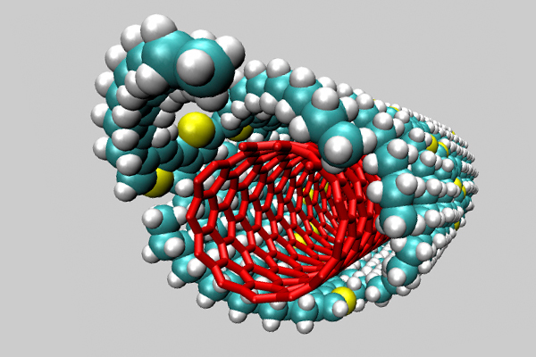 |
| Francois Gygi and Giulia Galli / UC-Davis A computer-generated cross section of the polymer-coated carbon nanotube. The polymer shell (blue) wraps around a semiconducting single-walled carbon nanotube (red). |
Abstract:
A new technique developed by Stanford researchers advances commercial potential of semiconducting carbon nanotubes for printable circuits, bendable display screens, stretchable electronics and solar technology.
Sorting out the nanotubes, for better electronics
Stanford, CA | Posted on November 18th, 2011BY SARAH JANE KELLER
Carbon nanotubes could make many electronic devices cheaper and more efficient. But when nanotubes are manufactured, tubes that work for solar cells are mixed with tubes that work for batteries. The final product is a nanotube powder that is not ideal for any single commercial application.
Zhenan Bao, Stanford associate professor of chemical engineering, and her colleagues at University of California-Davis and the Samsung Advanced Institute of Technology have discovered a technique to selectively sort semiconducting single-walled carbon nanotubes from the mixture. The results appear online in Nature Communications.
The semiconducting nanotubes could be used in flexible transistors for other technologies that Bao's group develops, including circuits printed on plastic, bendable display screens and stretchable electronics. The nanotubes could also close gaps in solar cell technology.
"Sorting has been a major bottleneck for carbon nanotubes to be viable for practical electronics applications," Bao said. "This work solves the problem of separating the conducting from the semiconducting nanotubes."
Conducting tubes are used in wires and electrodes but semiconducting tubes are the active material for transistors or solar cells. Mixtures of conducting and semiconducting tubes do not carry enough current for wires or battery electrodes. And when the mixture is used for semiconducting, as in a transistor, the excess current from the conducting nanotubes will short the device.
Bao's group uses a polymer that selectively sorts the mixture by wrapping around semiconducting nanotubes, and not conducting nanotubes. Mixing the polymer with commercially available carbon nanotubes in a solvent separates semiconducting tubes from conducting tubes.
In her past work with the polymer, Bao was the first to find that it has good semiconducting properties in transistors. It is now the most widely studied polymer for plastic circuits and plastic transistors and also for plastic solar cells. Bao's group is the first to combine it with semiconducting carbon nanotubes.
This is not the first time a polymer has been used to sort conducting and semiconducting nanotubes. However, past polymers have insulated the nanotubes and required extensive removal treatments to restore the conductivity of the nanotubes.
The polymer in Bao's process does not need to be removed. The final product is a semiconducting nanotube and polymer ink that can be used to make printable electronics.
"Our simple process allows us to build useful devices very easily," she said.
The group tested nearly 200 individual nanotubes to confirm that the polymer only wraps around semiconducting tubes and not conducting tubes. To explain how the polymer wraps around the carbon nanotube, UC-Davis collaborators Giulia Galli and Francois Gygi modeled the geometry of a semiconducting carbon nanotube and its polymer shell.
According to Galli, the model provides "a theoretical explanation of how this polymer actually interacts with the nanotube." The polymer has a long, rigid backbone, with regular arm-like molecular chains along each side. The side chains fit together like fingers, making a ribbon of polymer that wraps around the semiconducting nanotubes.
Bao's work with nanotubes is part of her long-term collaboration with the Samsung Advanced Institute of Technology. "I'm especially happy that this polymer can now be used to sort nanotubes," Bao said. "It merges two very important materials together and makes a hybrid material that could be very useful for printed and flexible electronics."
Jeffrey B.-H. Tok, senior research engineer; Andrew Spakowitz, assistant professor of chemical engineering; and H.S.Philip Wong, professor of electrical engineering, contributed to the research. Chemical engineering graduate student Hang Woo Lee, materials science and engineering graduate students Steve Park and Huiliang Wang also contributed, as well as Satoshi Morishita of chemical engineering,
Luckshitha S. Liyanage of electrical engineering and Nishant Patil of electrical engineering.
The Samsung Advanced Institute of Technology and the National Science Foundation provided funding for the research.
Sarah Jane Keller is a science-writing intern at the Stanford News Service.
####
For more information, please click here
Contacts:
Zhenan Bao
Department of Chemical Engineering
(650) 723-2419
Dan Stober
Stanford News Service:
(650) 721-6965
Copyright © Stanford University
If you have a comment, please Contact us.Issuers of news releases, not 7th Wave, Inc. or Nanotechnology Now, are solely responsible for the accuracy of the content.
Bookmark:


| Related News Press |
News and information
![]() Simulating magnetization in a Heisenberg quantum spin chain April 5th, 2024
Simulating magnetization in a Heisenberg quantum spin chain April 5th, 2024
![]() NRL charters Navy�s quantum inertial navigation path to reduce drift April 5th, 2024
NRL charters Navy�s quantum inertial navigation path to reduce drift April 5th, 2024
![]() Discovery points path to flash-like memory for storing qubits: Rice find could hasten development of nonvolatile quantum memory April 5th, 2024
Discovery points path to flash-like memory for storing qubits: Rice find could hasten development of nonvolatile quantum memory April 5th, 2024
![]() Good as gold - improving infectious disease testing with gold nanoparticles April 5th, 2024
Good as gold - improving infectious disease testing with gold nanoparticles April 5th, 2024
Display technology/LEDs/SS Lighting/OLEDs
![]() Utilizing palladium for addressing contact issues of buried oxide thin film transistors April 5th, 2024
Utilizing palladium for addressing contact issues of buried oxide thin film transistors April 5th, 2024
![]() Light guide plate based on perovskite nanocomposites November 3rd, 2023
Light guide plate based on perovskite nanocomposites November 3rd, 2023
![]() Simple ballpoint pen can write custom LEDs August 11th, 2023
Simple ballpoint pen can write custom LEDs August 11th, 2023
Flexible Electronics
![]() CityU awarded invention: Soft, ultrathin photonic material cools down wearable electronic devices June 30th, 2023
CityU awarded invention: Soft, ultrathin photonic material cools down wearable electronic devices June 30th, 2023
Chip Technology
![]() Discovery points path to flash-like memory for storing qubits: Rice find could hasten development of nonvolatile quantum memory April 5th, 2024
Discovery points path to flash-like memory for storing qubits: Rice find could hasten development of nonvolatile quantum memory April 5th, 2024
![]() Utilizing palladium for addressing contact issues of buried oxide thin film transistors April 5th, 2024
Utilizing palladium for addressing contact issues of buried oxide thin film transistors April 5th, 2024
![]() HKUST researchers develop new integration technique for efficient coupling of III-V and silicon February 16th, 2024
HKUST researchers develop new integration technique for efficient coupling of III-V and silicon February 16th, 2024
Nanotubes/Buckyballs/Fullerenes/Nanorods/Nanostrings
![]() Tests find no free-standing nanotubes released from tire tread wear September 8th, 2023
Tests find no free-standing nanotubes released from tire tread wear September 8th, 2023
![]() Detection of bacteria and viruses with fluorescent nanotubes July 21st, 2023
Detection of bacteria and viruses with fluorescent nanotubes July 21st, 2023
Nanoelectronics
![]() Interdisciplinary: Rice team tackles the future of semiconductors Multiferroics could be the key to ultralow-energy computing October 6th, 2023
Interdisciplinary: Rice team tackles the future of semiconductors Multiferroics could be the key to ultralow-energy computing October 6th, 2023
![]() Key element for a scalable quantum computer: Physicists from Forschungszentrum J�lich and RWTH Aachen University demonstrate electron transport on a quantum chip September 23rd, 2022
Key element for a scalable quantum computer: Physicists from Forschungszentrum J�lich and RWTH Aachen University demonstrate electron transport on a quantum chip September 23rd, 2022
![]() Reduced power consumption in semiconductor devices September 23rd, 2022
Reduced power consumption in semiconductor devices September 23rd, 2022
![]() Atomic level deposition to extend Moore�s law and beyond July 15th, 2022
Atomic level deposition to extend Moore�s law and beyond July 15th, 2022
Discoveries
![]() Chemical reactions can scramble quantum information as well as black holes April 5th, 2024
Chemical reactions can scramble quantum information as well as black holes April 5th, 2024
![]() New micromaterial releases nanoparticles that selectively destroy cancer cells April 5th, 2024
New micromaterial releases nanoparticles that selectively destroy cancer cells April 5th, 2024
![]() Utilizing palladium for addressing contact issues of buried oxide thin film transistors April 5th, 2024
Utilizing palladium for addressing contact issues of buried oxide thin film transistors April 5th, 2024
Announcements
![]() NRL charters Navy�s quantum inertial navigation path to reduce drift April 5th, 2024
NRL charters Navy�s quantum inertial navigation path to reduce drift April 5th, 2024
![]() Discovery points path to flash-like memory for storing qubits: Rice find could hasten development of nonvolatile quantum memory April 5th, 2024
Discovery points path to flash-like memory for storing qubits: Rice find could hasten development of nonvolatile quantum memory April 5th, 2024
Energy
![]() Development of zinc oxide nanopagoda array photoelectrode: photoelectrochemical water-splitting hydrogen production January 12th, 2024
Development of zinc oxide nanopagoda array photoelectrode: photoelectrochemical water-splitting hydrogen production January 12th, 2024
![]() Shedding light on unique conduction mechanisms in a new type of perovskite oxide November 17th, 2023
Shedding light on unique conduction mechanisms in a new type of perovskite oxide November 17th, 2023
![]() Inverted perovskite solar cell breaks 25% efficiency record: Researchers improve cell efficiency using a combination of molecules to address different November 17th, 2023
Inverted perovskite solar cell breaks 25% efficiency record: Researchers improve cell efficiency using a combination of molecules to address different November 17th, 2023
![]() The efficient perovskite cells with a structured anti-reflective layer � another step towards commercialization on a wider scale October 6th, 2023
The efficient perovskite cells with a structured anti-reflective layer � another step towards commercialization on a wider scale October 6th, 2023
Solar/Photovoltaic
![]() Development of zinc oxide nanopagoda array photoelectrode: photoelectrochemical water-splitting hydrogen production January 12th, 2024
Development of zinc oxide nanopagoda array photoelectrode: photoelectrochemical water-splitting hydrogen production January 12th, 2024
![]() Shedding light on unique conduction mechanisms in a new type of perovskite oxide November 17th, 2023
Shedding light on unique conduction mechanisms in a new type of perovskite oxide November 17th, 2023
![]() Inverted perovskite solar cell breaks 25% efficiency record: Researchers improve cell efficiency using a combination of molecules to address different November 17th, 2023
Inverted perovskite solar cell breaks 25% efficiency record: Researchers improve cell efficiency using a combination of molecules to address different November 17th, 2023
![]() Charged �molecular beasts� the basis for new compounds: Researchers at Leipzig University use �aggressive� fragments of molecular ions for chemical synthesis November 3rd, 2023
Charged �molecular beasts� the basis for new compounds: Researchers at Leipzig University use �aggressive� fragments of molecular ions for chemical synthesis November 3rd, 2023
Printing/Lithography/Inkjet/Inks/Bio-printing/Dyes
![]() Presenting: Ultrasound-based printing of 3D materials�potentially inside the body December 8th, 2023
Presenting: Ultrasound-based printing of 3D materials�potentially inside the body December 8th, 2023
![]() Simple ballpoint pen can write custom LEDs August 11th, 2023
Simple ballpoint pen can write custom LEDs August 11th, 2023
![]() Disposable electronics on a simple sheet of paper October 7th, 2022
Disposable electronics on a simple sheet of paper October 7th, 2022
|
|
||
|
|
||
| The latest news from around the world, FREE | ||
|
|
||
|
|
||
| Premium Products | ||
|
|
||
|
Only the news you want to read!
Learn More |
||
|
|
||
|
Full-service, expert consulting
Learn More |
||
|
|
||