Home > Press > Graphene and friends: A new method to make 2D materials
 |
| http://dx.doi.org/10.1002/anie.201106004|Z. Zeng, Angew. Chem. Int. Ed. ; DOI: 10.1002/anie.201106004 |
Abstract:
by Adrian Miller
Although graphene has had materials researcher hearts racing more or less since its discovery, many scientists see it as just the beginning - if other materials could be processed in the same way, they ask, couldn't it mean a revolution in nanodevice design? Imagine a range of two-dimensional materials, each with their own unique thermal, electronic, optical, and mechanical properties, used for a whole host of nanotechnology applications.
Graphene and friends: A new method to make 2D materials
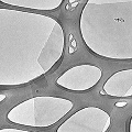
Germany | Posted on November 10th, 2011The problem with this vision - at least, up until now - is that graphene is the only 2D material that can be reliably and easily synthesized in large enough quantities to be useful for device manufacture. Other compounds, for example MoS2 and WS2, are right up there with graphite in terms of potential, but the groups working on their processing haven't been able to move past small scale methods such as mechanical cleavage (� la Geim and Novoselov) and nanotube "unzipping".
However, that might be about to change - last week, a Singaporean team reported a new process to create large numbers of single-layer nanosheets quickly and efficiently, applicable to any suitable bulk material. By inducing lithiation with an electrochemical setup, the materials can be carefully monitored and put into a state ideal for ultrasonication and exfoliation. In less than six hours, and at room temperatures, their test setup obtained an MoS2 nanosheet yield of 92%.
To demonstrate how useful these sheets could be, the team went on to create a proof-of-concept nitric oxide detector from these single MoS2 layers. As they're electrically conductive over large areas, and act as p-type semiconductors, they respond electronically to different NO concentrations, and the addition of gold electrodes meant that the response could measured. This experimental device showed great promise - a detection limit of 190 ppt, definitely well within the limits for a promising sensing platform.
Other, similar, experiments yielded similar results with WS2, TiS2, and others - even graphene! - and the researchers see their method as one that could be adopted to produce a range of 2D nanosheets, for application in areas such as electronics, catalysis, and sensing.
####
For more information, please click here
Copyright © Wiley-VCH Materials Science Journals
If you have a comment, please Contact us.Issuers of news releases, not 7th Wave, Inc. or Nanotechnology Now, are solely responsible for the accuracy of the content.
Bookmark:


| Related News Press |
News and information
![]() Simulating magnetization in a Heisenberg quantum spin chain April 5th, 2024
Simulating magnetization in a Heisenberg quantum spin chain April 5th, 2024
![]() NRL charters Navy�s quantum inertial navigation path to reduce drift April 5th, 2024
NRL charters Navy�s quantum inertial navigation path to reduce drift April 5th, 2024
![]() Discovery points path to flash-like memory for storing qubits: Rice find could hasten development of nonvolatile quantum memory April 5th, 2024
Discovery points path to flash-like memory for storing qubits: Rice find could hasten development of nonvolatile quantum memory April 5th, 2024
Chemistry
![]() What heat can tell us about battery chemistry: using the Peltier effect to study lithium-ion cells March 8th, 2024
What heat can tell us about battery chemistry: using the Peltier effect to study lithium-ion cells March 8th, 2024
![]() Nanoscale CL thermometry with lanthanide-doped heavy-metal oxide in TEM March 8th, 2024
Nanoscale CL thermometry with lanthanide-doped heavy-metal oxide in TEM March 8th, 2024
Graphene/ Graphite
![]() NRL discovers two-dimensional waveguides February 16th, 2024
NRL discovers two-dimensional waveguides February 16th, 2024
Chip Technology
![]() Discovery points path to flash-like memory for storing qubits: Rice find could hasten development of nonvolatile quantum memory April 5th, 2024
Discovery points path to flash-like memory for storing qubits: Rice find could hasten development of nonvolatile quantum memory April 5th, 2024
![]() Utilizing palladium for addressing contact issues of buried oxide thin film transistors April 5th, 2024
Utilizing palladium for addressing contact issues of buried oxide thin film transistors April 5th, 2024
![]() HKUST researchers develop new integration technique for efficient coupling of III-V and silicon February 16th, 2024
HKUST researchers develop new integration technique for efficient coupling of III-V and silicon February 16th, 2024
Sensors
Discoveries
![]() Chemical reactions can scramble quantum information as well as black holes April 5th, 2024
Chemical reactions can scramble quantum information as well as black holes April 5th, 2024
![]() New micromaterial releases nanoparticles that selectively destroy cancer cells April 5th, 2024
New micromaterial releases nanoparticles that selectively destroy cancer cells April 5th, 2024
![]() Utilizing palladium for addressing contact issues of buried oxide thin film transistors April 5th, 2024
Utilizing palladium for addressing contact issues of buried oxide thin film transistors April 5th, 2024
Announcements
![]() NRL charters Navy�s quantum inertial navigation path to reduce drift April 5th, 2024
NRL charters Navy�s quantum inertial navigation path to reduce drift April 5th, 2024
![]() Discovery points path to flash-like memory for storing qubits: Rice find could hasten development of nonvolatile quantum memory April 5th, 2024
Discovery points path to flash-like memory for storing qubits: Rice find could hasten development of nonvolatile quantum memory April 5th, 2024
|
|
||
|
|
||
| The latest news from around the world, FREE | ||
|
|
||
|
|
||
| Premium Products | ||
|
|
||
|
Only the news you want to read!
Learn More |
||
|
|
||
|
Full-service, expert consulting
Learn More |
||
|
|
||