Home > Press > Study Compares Fundamental Techniques for Doping Graphene Sheets
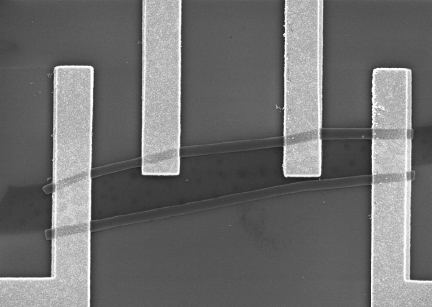 |
| SEM image of doping study
Georgia Institute of Technology |
Abstract:
Nanotechnology researchers at the Georgia Institute of Technology have conducted the first direct comparison of two fundamental techniques that could be used for chemically doping sheets of two-dimensional graphene for the fabrication of devices and interconnects.
Study Compares Fundamental Techniques for Doping Graphene Sheets
Atlanta, GA | Posted on November 7th, 2011Chemical doping is routinely used in conventional three-dimensional semiconductors to control the density of electron carriers that are essential to the operation of devices such as transistors. But graphene, a semi-metal available in sheets just one atom thick, has properties very different from traditional materials such as silicon -- though researchers say doping will still be needed for producing electronic devices.
The bad news is that electronic designers working with graphene won't be able to simply apply what they've been doing with three-dimensional semiconductors -- which would translate to vastly degraded material quality for graphene. The good news, according to the study, is that graphene doping can be combined with other processes -- and need be applied only to the edges of nanoscale structures being fabricated.
"We are learning how to manipulate these two-dimensional sheets of carbon atoms to get some very unusual results that aren't available with any other material," said James Meindl, director of Georgia Tech's Nanotechnology Research Center, where the research was conducted. "Doping graphene to try to influence its properties is important to being able to use it effectively."
Details of the research were published online in the journal Carbon on October 29th. The research was supported by the Semiconductor Research Corporation (SRC), the Defense Advanced Research Projects Agency (DARPA) through the Interconnect Focus Center, and the National Science Foundation (NSF).
Because graphene sheets contain so few atoms by area, the substitution of elements such as oxygen or nitrogen for carbon atoms in the lattice -- as in conventional doping -- detracts from the high electron mobility and other properties that make the material interesting. So the researchers are rethinking the doping process to take advantage of graphene's unique properties.
"When we work with a three-dimensional semiconductor, we embed the dopant species in the bulk material and then fabricate it into a device," said Kevin Brenner, a graduate research assistant in the Georgia Tech School of Electrical and Computer Engineering. "With graphene, we will dope the material as we process it and fabricate it into devices or interconnects. Doping may be done as part of other fabrication steps such as plasma etching, and that will require us to reinvent the whole process."
Using sheets of exfoliated graphene, Brenner and collaborators Raghu Murali and Yinxiao Yang evaluated the effectiveness of two different techniques: edge passivation by coupling electron-beam lithography with a common resist material, and adsorption from coating the surface of the material. They found that the edge treatment, which chemically reacts with defects created when the material is cut, was a thousand times more efficient at producing carriers in the graphene sheets than the surface treatment.
"We will only be working with the edges of the material," Brenner explained. "That will allow us to leave the center pristine and free of defects. Using this approach, we can maintain very high mobilities and the special properties of graphene while creating very high carrier densities."
Because of the two-dimensional nature of the graphene, controlling the edge chemistry can provide control over the bulk properties of the sheet. "At nanoscale dimensions, the edge atoms tend to dominate over surface adsorption techniques," he added. "With a seven nanometer by seven nanometer graphene device, passivating just one edge C-atom provides the doping equivalent of covering the entire surface."
For doping the edge of a graphene structure, the team applied a thin film of hydrogen silsesquioxane (HSQ), a chemical normally used as a resist for etching, then used electron beam lithography to cross-link the material, which added oxygen atoms to the edges to create p-type doping. The resist and electron beam system combined to provide nanometer-scale control over where the chemical changes took place.
Doping treatment could also be applied using plasma etching, Brenner said. Controlling the specific atoms used in the plasma, or conducting the etching process in an environment containing specific atoms, could drive those atoms into the edges where they would serve as dopants.
"Anytime you create an edge, you have created a location where you can passivate using a dopant," he added. "Instead of needing to embed it in the surface, you can just take the edge that is already there and passivate it with oxygen, nitrogen, hydrogen or other dopant. It could be almost an effortless process because the doping can be done as part of another step."
Beyond fabricating electronic devices, Nanotechnology Research Center scientists are interested in using graphene for interconnects, potentially as a replacement for copper. As interconnect structures become smaller and smaller, the resistivity of copper increases. Edge-doped graphene sheets exhibit a trend of increasing doping with reduced dimensions, possibly becoming more conductive as their size shrinks below 50 nanometers, making them attractive for nanoscale interconnects.
Armed with basic information about graphene doping, the researchers hope to now begin producing devices to study how graphene actually performs.
"Now that we have made a start at understanding how to dope the material, the next step is to begin putting this into nanoscale devices," Brenner said. "We want to see what kind of performance we can get. That may tell us where graphene's niche could be as an electronic material."
Meindl, who has worked with silicon since the dawn of integrated circuits, says it's too early to predict where graphene will ultimately find commercial applications. But he says the material's properties are too interesting not to explore.
"The chances are that something very interesting and unique will develop from the use of graphene," he said. "But we don't yet have the ability to predict what we will be able to do with this new material."
Writer: John Toon
####
For more information, please click here
Contacts:
Research News & Publications Office
Georgia Institute of Technology
75 Fifth Street, N.W., Suite 314
Atlanta, Georgia 30308 USA
Media Relations Contacts:
John Toon
404-894-6986
or
Abby Robinson
404-385-3364
Copyright © Georgia Institute of Technology
If you have a comment, please Contact us.Issuers of news releases, not 7th Wave, Inc. or Nanotechnology Now, are solely responsible for the accuracy of the content.
Bookmark:


| Related Links |
![]() Nanotechnology Research Center:
Nanotechnology Research Center:
![]() School of Electrical and Computer Engineering:
School of Electrical and Computer Engineering:
| Related News Press |
News and information
![]() Simulating magnetization in a Heisenberg quantum spin chain April 5th, 2024
Simulating magnetization in a Heisenberg quantum spin chain April 5th, 2024
![]() NRL charters Navy�s quantum inertial navigation path to reduce drift April 5th, 2024
NRL charters Navy�s quantum inertial navigation path to reduce drift April 5th, 2024
![]() Discovery points path to flash-like memory for storing qubits: Rice find could hasten development of nonvolatile quantum memory April 5th, 2024
Discovery points path to flash-like memory for storing qubits: Rice find could hasten development of nonvolatile quantum memory April 5th, 2024
Graphene/ Graphite
![]() NRL discovers two-dimensional waveguides February 16th, 2024
NRL discovers two-dimensional waveguides February 16th, 2024
Chip Technology
![]() Discovery points path to flash-like memory for storing qubits: Rice find could hasten development of nonvolatile quantum memory April 5th, 2024
Discovery points path to flash-like memory for storing qubits: Rice find could hasten development of nonvolatile quantum memory April 5th, 2024
![]() Utilizing palladium for addressing contact issues of buried oxide thin film transistors April 5th, 2024
Utilizing palladium for addressing contact issues of buried oxide thin film transistors April 5th, 2024
![]() HKUST researchers develop new integration technique for efficient coupling of III-V and silicon February 16th, 2024
HKUST researchers develop new integration technique for efficient coupling of III-V and silicon February 16th, 2024
Discoveries
![]() Chemical reactions can scramble quantum information as well as black holes April 5th, 2024
Chemical reactions can scramble quantum information as well as black holes April 5th, 2024
![]() New micromaterial releases nanoparticles that selectively destroy cancer cells April 5th, 2024
New micromaterial releases nanoparticles that selectively destroy cancer cells April 5th, 2024
![]() Utilizing palladium for addressing contact issues of buried oxide thin film transistors April 5th, 2024
Utilizing palladium for addressing contact issues of buried oxide thin film transistors April 5th, 2024
Announcements
![]() NRL charters Navy�s quantum inertial navigation path to reduce drift April 5th, 2024
NRL charters Navy�s quantum inertial navigation path to reduce drift April 5th, 2024
![]() Discovery points path to flash-like memory for storing qubits: Rice find could hasten development of nonvolatile quantum memory April 5th, 2024
Discovery points path to flash-like memory for storing qubits: Rice find could hasten development of nonvolatile quantum memory April 5th, 2024
|
|
||
|
|
||
| The latest news from around the world, FREE | ||
|
|
||
|
|
||
| Premium Products | ||
|
|
||
|
Only the news you want to read!
Learn More |
||
|
|
||
|
Full-service, expert consulting
Learn More |
||
|
|
||