Home > Press > A SHARP New Microscope for the Next Generation of Microchips: Berkeley Lab scientists and colleagues will create an advanced extreme-ultraviolet microscope
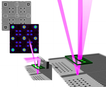 |
| At top are programmed pattern defects, including the large protrusion in the center, developed by a team at IBM to evaluate printing sensitivity. The current AIT microscope�s image of the defects is center left. The final stage of the AIT�s beam path is shown bottom left: the synchrotron�s EUV beam enters from the top, reflects from the mask, is focused by an array of zone plates, and then reflects from a turning mirror to an EUV-sensitive camera, not shown, to the left. The more efficient SHARP beam path at right removes the turning mirror and a window from the array of zone plates to increase brightness. SHARP incorporates other refinements such as a new high-efficiency illuminator, a tunable monochromator that controls the coherence of the light, and a choice of zone plate lenses for different magnifications as the microscope navigates around the mask. |
Abstract:
Moore's Law, hardly a law but undeniably a persistent trend, says that every year and a half, the number of transistors that fit on a chip roughly doubles. It's why electronics - from smart phones to flat screens, from MP4 players to movie cameras, from tablets to supercomputers - grow ever more varied, powerful, and compact, but also ever less expensive. Whether the trend can continue until it runs up against immutable laws of nature, like the finite size of an atom, depends on how far scientists and technicians can push electronic technologies down into the nanoworld with better tools for using short-wavelength light.
A SHARP New Microscope for the Next Generation of Microchips: Berkeley Lab scientists and colleagues will create an advanced extreme-ultraviolet microscope
Berkeley, CA | Posted on November 1st, 2011Now scientists at the U.S. Department of Energy's Lawrence Berkeley National Laboratory (Berkeley Lab) have partnered with colleagues at leading semiconductor manufacturers to create the world's most advanced extreme-ultraviolet (EUV) microscope. Called SHARP (a succinct acronym for a long name, the Semiconductor High-NA Actinic Reticle Review Project), the new microscope will be dedicated to photolithography, the central process in the creation of computer chips.
The $4.1 million, 1.5-year project will be led by Kenneth Goldberg of the Center for X-Ray Optics (CXRO) in Berkeley Lab's Materials Science Division (MSD). Initially SHARP will be used in parallel with operations at the existing microscope on beamline 11.3.2 of Berkeley Lab's Advanced Light Source (ALS). By the last quarter of 2012 the new EUV photomask-imaging microscope will replace the beamline's aging facilities.
"EUV light is tricky to work with," says Goldberg, "because every material absorbs it so strongly. So instead of glass lenses, EUV optical systems rely mainly on specialized mirrors with atomic-scale smoothness, topped by multilayer coatings for high reflectivity." To maintain efficiency, the entire optical system has to be placed in a high-vacuum environment.
While the existing eight-year-old microscope at beamline 11.3.2, dubbed the AIT (for Actinic Inspection Tool), has unique imaging capabilities, the fast-moving nature of semiconductor technology means its future is limited. SHARP will exceed its performance in every metric: resolution, speed, uniformity of illumination, and coherence control. SHARP will enable forward-looking research years before commercial tools become available.
Within a few years, semiconductor devices will be measured in dimensions of 16, 11, or 8 nanometers, mere billionths of a meter. To mass-produce them, industry is pushing a photolithography process that uses EUV light with a wavelength of just 13.5 nanometers, 40 times smaller than visible light.
"At this short wavelength, we can print and image circuit patterns at nanometer length scales," says Goldberg. "The new microscope will leverage years of cutting-edge EUV and soft-x‑ray microscopy experience, experimental systems-engineering at CXRO, and EUV optics expertise developed as part of the lithography research programs here." Goldberg says that the ALS, as one of the world's brightest sources of EUV light, "is a great place to develop EUV lithography technologies."
In lithography, photomasks are the key to mass production. A series of photomasks carry the master circuit patterns that are transferred onto a chip, layer by layer, to create working semiconductor devices. The masks are analogous to the negatives in a photographer's darkroom, or master pages on a photocopier.
Minute imperfections or tiny particles of dust on a master, if not found and cleaned or fixed, ultimately cause chips to fail. Goldberg and his team have shown that defects and patterns can appear very different when viewed with non-EUV inspection tools such as electron microscopes, making EUV microscopy essential for the development of EUV masks because only in this way can damaging dust particles and other defects be identified reliably.
"Other microscopes can have wonderfully high resolution, but they can't detect the wavelength-specific EUV response of mask patterns and defects," says Goldberg, "and that's necessary to make successful repairs."
SHARP is called an "actinic" microscope because it uses the same EUV wavelengths used in production. Thus the new EUV microscope will enable semiconductor company researchers to better evaluate defects and repair strategies, mask materials and architectures, and advanced pattern features.
Like its predecessor, the SHARP microscope will also feature an array of lenses, side by side, so users can select the different imaging properties they need, much as a common lab microscope mounts different lenses on a rotating turret.
The high-magnification objective lenses for the new microscope are holographic Fresnel zoneplate lenses, microscopic objects produced by CXRO's Nanowriter. The Nanowriter, under the direction of Erik Anderson, holds the world record for creating the highest resolution zoneplates for many synchrotron and other short-wavelength applications. The lenses are only slightly wider than a single human hair, yet they project high-quality images of the mask surface with up to 2,000 times magnification.
A special feature of the new microscope will be illumination coherence control. The ALS produces an EUV beam with laser-like coherence, ideal for many experiments. For microscopy, however, the image resolution can be improved by a factor of two by carefully re-engineering the illumination into a state called partial coherence. Microscopists have recognized the importance of partial coherence for years, and the synchrotron community is now catching up.
An angle-scanning mirror in the new microscope's beamline illuminator will take the highly-coherent ALS light and steer it into patterns, like a mini-laser-light show, breaking and re-shaping the coherence properties. In this way, the SHARP microscope will replicate the properties of current and future tools for lithography production and research, giving researchers the most advanced look at what's to come.
Additional information
With sales of some $51 billion a year, semiconductors are the United States' second largest export product. Developing technology to produce and test the next generation computer chips is one of the industry's core missions. For over a decade, semiconductor companies have sponsored photolithography-related research at Berkeley Lab through the Center for X-Ray Optics, including world-leading programs in optics, masks, and materials � most conducted on three CXRO beamlines at the Advanced Light Source. For more information on CXRO, visit www.cxro.lbl.gov/. For more information on the ALS visit www-als.lbl.gov/.
####
About Berkeley Lab
Lawrence Berkeley National Laboratory addresses the world�s most urgent scientific challenges by advancing sustainable energy, protecting human health, creating new materials, and revealing the origin and fate of the universe. Founded in 1931, Berkeley Lab�s scientific expertise has been recognized with 13 Nobel prizes. The University of California manages Berkeley Lab for the U.S. Department of Energy�s Office of Science. For more, visit www.lbl.gov.
For more information, please click here
Contacts:
Paul Preuss
510-486-6249
Copyright © Berkeley Lab
If you have a comment, please Contact us.Issuers of news releases, not 7th Wave, Inc. or Nanotechnology Now, are solely responsible for the accuracy of the content.
Bookmark:


| Related News Press |
News and information
![]() Simulating magnetization in a Heisenberg quantum spin chain April 5th, 2024
Simulating magnetization in a Heisenberg quantum spin chain April 5th, 2024
![]() NRL charters Navy�s quantum inertial navigation path to reduce drift April 5th, 2024
NRL charters Navy�s quantum inertial navigation path to reduce drift April 5th, 2024
![]() Discovery points path to flash-like memory for storing qubits: Rice find could hasten development of nonvolatile quantum memory April 5th, 2024
Discovery points path to flash-like memory for storing qubits: Rice find could hasten development of nonvolatile quantum memory April 5th, 2024
Imaging
![]() Nanoscale CL thermometry with lanthanide-doped heavy-metal oxide in TEM March 8th, 2024
Nanoscale CL thermometry with lanthanide-doped heavy-metal oxide in TEM March 8th, 2024
Laboratories
![]() A battery�s hopping ions remember where they�ve been: Seen in atomic detail, the seemingly smooth flow of ions through a battery�s electrolyte is surprisingly complicated February 16th, 2024
A battery�s hopping ions remember where they�ve been: Seen in atomic detail, the seemingly smooth flow of ions through a battery�s electrolyte is surprisingly complicated February 16th, 2024
![]() NRL discovers two-dimensional waveguides February 16th, 2024
NRL discovers two-dimensional waveguides February 16th, 2024
Govt.-Legislation/Regulation/Funding/Policy
![]() NRL charters Navy�s quantum inertial navigation path to reduce drift April 5th, 2024
NRL charters Navy�s quantum inertial navigation path to reduce drift April 5th, 2024
![]() Discovery points path to flash-like memory for storing qubits: Rice find could hasten development of nonvolatile quantum memory April 5th, 2024
Discovery points path to flash-like memory for storing qubits: Rice find could hasten development of nonvolatile quantum memory April 5th, 2024
![]() Chemical reactions can scramble quantum information as well as black holes April 5th, 2024
Chemical reactions can scramble quantum information as well as black holes April 5th, 2024
Announcements
![]() NRL charters Navy�s quantum inertial navigation path to reduce drift April 5th, 2024
NRL charters Navy�s quantum inertial navigation path to reduce drift April 5th, 2024
![]() Discovery points path to flash-like memory for storing qubits: Rice find could hasten development of nonvolatile quantum memory April 5th, 2024
Discovery points path to flash-like memory for storing qubits: Rice find could hasten development of nonvolatile quantum memory April 5th, 2024
Tools
![]() Ferroelectrically modulate the Fermi level of graphene oxide to enhance SERS response November 3rd, 2023
Ferroelectrically modulate the Fermi level of graphene oxide to enhance SERS response November 3rd, 2023
![]() The USTC realizes In situ electron paramagnetic resonance spectroscopy using single nanodiamond sensors November 3rd, 2023
The USTC realizes In situ electron paramagnetic resonance spectroscopy using single nanodiamond sensors November 3rd, 2023
Photonics/Optics/Lasers
![]() With VECSELs towards the quantum internet Fraunhofer: IAF achieves record output power with VECSEL for quantum frequency converters April 5th, 2024
With VECSELs towards the quantum internet Fraunhofer: IAF achieves record output power with VECSEL for quantum frequency converters April 5th, 2024
![]() Nanoscale CL thermometry with lanthanide-doped heavy-metal oxide in TEM March 8th, 2024
Nanoscale CL thermometry with lanthanide-doped heavy-metal oxide in TEM March 8th, 2024
![]() Optically trapped quantum droplets of light can bind together to form macroscopic complexes March 8th, 2024
Optically trapped quantum droplets of light can bind together to form macroscopic complexes March 8th, 2024
![]() HKUST researchers develop new integration technique for efficient coupling of III-V and silicon February 16th, 2024
HKUST researchers develop new integration technique for efficient coupling of III-V and silicon February 16th, 2024
|
|
||
|
|
||
| The latest news from around the world, FREE | ||
|
|
||
|
|
||
| Premium Products | ||
|
|
||
|
Only the news you want to read!
Learn More |
||
|
|
||
|
Full-service, expert consulting
Learn More |
||
|
|
||