Home > Press > State-of-the-art integrated IR-UWB enabling global high-quality low-power mobile applications
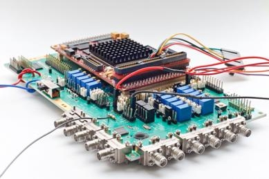 |
| Imec�s and Holst Centre�s fully chip-integrated ultralow-power IR-UWB (impulse-radio ultra-wideband) solution |
Abstract:
Imec and Holst Centre present a fully chip-integrated ultralow-power IR-UWB (impulse-radio ultra-wideband) solution for use in the worldwide available 6-10GHz band. The radio delivers high-quality communication for battery-operated mobile and sensing applications. It operates fade-resilient and interference-free.
State-of-the-art integrated IR-UWB enabling global high-quality low-power mobile applications
Leuven, Belgium | Posted on October 11th, 2011With its first ultralow-power integrated solution for the 6-10GHz band, imec and Holst Centre now make UWB communication available for battery-operated applications in the area of personal area networks and positioning sensors worldwide. Examples are short-range video streaming or around-the-body audio streaming (e.g. between a headset and a smartphone). When using the UWB radio for the wireless streaming of audio between for example a smartphone and an earpiece, the battery lifetime of the smartphone will increase by over 3x compared to a conventional Bluetooth-based solution, and the earpiece will have a battery lifetime increase of over 5x. In contrast to the Bluetooth communication, the UWB radio will not suffer from interference from other wireless technologies that operate in the same location and in the same frequency band.
Impulse ultra-wideband communication is especially suited for short-range (20m) communication and positioning sensors. The large bandwidth improves the resilience against fades, resulting in a superior communication reliability. This is especially so compared to narrowband solutions, which tend to lose signals in surroundings with reflective surfaces and multi-path propagation. Also, spreading information over a wide bandwidth decreases the power spectral density, thus reducing the interference with other systems and lowering the probability of interception. IR-UWB is also suitable for positioning sensors; the reflection of the wide-band signal allows for centimeter-ranging positioning accuracy.
Imec and Holst Centre's solution consists of a transmitter, receiver front-end, and receiver digital baseband. The transmitter delivers 13dBm peak power, with an average power consumption of 3.3mW. The receiver front-end shows -88dBm sensitivity at 1Mbps. A digital synchronization algorithm enables real-time duty cycling, resulting in a mean power consumption of 3mW. A DCO with 100ppm frequency accuracy and a baseband frequency tracking algorithm ensure the coherent reception. A 75dB link budget with a data rate of 1Mbps is achieved.
Companies can have access to this technology by joining imec and Holst Centre's R&D program on ultra-low power wireless systems.
####
About IMEC
Imec performs world-leading research in nanoelectronics. Imec leverages its scientific knowledge with the innovative power of its global partnerships in ICT, healthcare and energy. Imec delivers industry-relevant technology solutions. In a unique high-tech environment, its international top talent is committed to providing the building blocks for a better life in a sustainable society. Imec is headquartered in Leuven, Belgium, and has offices in Belgium, the Netherlands, Taiwan, US, China, India and Japan. Its staff of about 1,900 people includes more than 500 industrial residents and guest researchers. In 2010, imec's revenue (P&L) was 285 million euro. Further information on imec can be found at www.imec.be.
Imec is a registered trademark for the activities of IMEC International (a legal entity set up under Belgian law as a "stichting van openbaar nut�), imec Belgium (IMEC vzw supported by the Flemish Government), imec the Netherlands (Stichting IMEC Nederland, part of Holst Centre which is supported by the Dutch Government), imec Taiwan (IMEC Taiwan Co.) and imec China (IMEC Microelectronics (Shangai) Co. Ltd.) and imec India (Imec India Private Limited).
About Holst Centre
Holst Centre is an independent open-innovation R&D centre that develops generic technologies for Wireless Autonomous Transducer Solutions and for Systems-in-Foil. A key feature of Holst Centre is its partnership model with industry and academia around shared roadmaps and programs. It is this kind of cross-fertilization that enables Holst Centre to tune its scientific strategy to industrial needs.
Holst Centre was set up in 2005 by imec (Flanders, Belgium) and TNO (The Netherlands) with support from the Dutch Ministry of Economic Affairs and the Government of Flanders. It is named after Gilles Holst, a Dutch pioneer in Research and Development and first director of Philips Research.
Located on High Tech Campus Eindhoven, Holst Centre benefits from the state-of-the-art on-site facilities. Holst Centre has over 150 employees from around 25 nationalities and a commitment from more than 30 industrial partners. Visit us at www.holstcentre.com
For more information, please click here
Contacts:
Hanne Degans
External Communications Officer
T: +32 16 28 17 69
M: +32 486 065 175
Barbara Kalkis
Maestro Marketing & PR
T : +1 408 996 9975
Copyright © IMEC
If you have a comment, please Contact us.Issuers of news releases, not 7th Wave, Inc. or Nanotechnology Now, are solely responsible for the accuracy of the content.
Bookmark:


| Related News Press |
News and information
![]() Simulating magnetization in a Heisenberg quantum spin chain April 5th, 2024
Simulating magnetization in a Heisenberg quantum spin chain April 5th, 2024
![]() NRL charters Navy�s quantum inertial navigation path to reduce drift April 5th, 2024
NRL charters Navy�s quantum inertial navigation path to reduce drift April 5th, 2024
![]() Discovery points path to flash-like memory for storing qubits: Rice find could hasten development of nonvolatile quantum memory April 5th, 2024
Discovery points path to flash-like memory for storing qubits: Rice find could hasten development of nonvolatile quantum memory April 5th, 2024
Chip Technology
![]() Discovery points path to flash-like memory for storing qubits: Rice find could hasten development of nonvolatile quantum memory April 5th, 2024
Discovery points path to flash-like memory for storing qubits: Rice find could hasten development of nonvolatile quantum memory April 5th, 2024
![]() Utilizing palladium for addressing contact issues of buried oxide thin film transistors April 5th, 2024
Utilizing palladium for addressing contact issues of buried oxide thin film transistors April 5th, 2024
![]() HKUST researchers develop new integration technique for efficient coupling of III-V and silicon February 16th, 2024
HKUST researchers develop new integration technique for efficient coupling of III-V and silicon February 16th, 2024
Announcements
![]() NRL charters Navy�s quantum inertial navigation path to reduce drift April 5th, 2024
NRL charters Navy�s quantum inertial navigation path to reduce drift April 5th, 2024
![]() Discovery points path to flash-like memory for storing qubits: Rice find could hasten development of nonvolatile quantum memory April 5th, 2024
Discovery points path to flash-like memory for storing qubits: Rice find could hasten development of nonvolatile quantum memory April 5th, 2024
|
|
||
|
|
||
| The latest news from around the world, FREE | ||
|
|
||
|
|
||
| Premium Products | ||
|
|
||
|
Only the news you want to read!
Learn More |
||
|
|
||
|
Full-service, expert consulting
Learn More |
||
|
|
||