Home > Press > Imec demonstrates extremely high-speed heterojunction bipolar transistors: The devices open new avenues in wireless communications and imaging
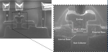 |
| Cross-section of bipolar HBT device in a B-E-B-C configuration after end-of-line processing |
Abstract:
Imec realized a fT/fMAX 245GHz/450GHz SiGe:C heterojunction bipolar transistor (HBT) device, a key enabler for future high-volume millimeter-wave low-power circuits to be used in automotive radar applications. These HBT devices also pave the way to silicon-based millimeter wave circuits penetrating the so-called THz gap, enabling enhanced imaging systems for security, medical and scientific applications
Imec demonstrates extremely high-speed heterojunction bipolar transistors: The devices open new avenues in wireless communications and imaging
Leuven, Belgium | Posted on October 10th, 2011The extremely high-speed devices have a fully self-aligned architecture by self-alignment of the emitter, base and collector region, and implement an optimized collector doping profile. Compared to III-V HBT devices, SiGe:C HBTs combine high-density and low-cost integration, making them suitable for consumer applications. Such high-speed devices can open up new application areas, working at very high frequencies with lower power dissipation, or applications which require a reduced impact of process, voltage and temperature variations at lower frequencies for better circuit reliability.
To achieve the ultra high-speed requirements, state-of-the-art SiGe:C HBTs need further up-scaling of the device performance. Thin sub-collector doping profiles are generally believed to be mandatory for this up-scaling. Usually, the collector dopants are introduced in the beginning of the processing and thus exposed to the complete thermal budget of the process flow. This complicates the accurate positioning of the buried collector. By in-situ arsenic doping during the simultaneous growth of the sub-collector pedestal and the SiGe:C base, imec introduced both a thin, well controlled, lowly doped collector region close to the base and a sharp transition to the highly doped collector without further complicating the process. This resulted in a considerable increase of the overall HBT device performance: Peak fMAX values above 450GHz are obtained on devices with a high early voltage, a BVCEO of 1.7V and a sharp transition from the saturation to the active region in the IC-VCE output curve. Despite the aggressive scaling of the sub-collector doping profile, the collector-base capacitance values did not increase much. Moreover, the current gain is well defined, with an average around 400 and the emitter-base tunnel current, visible at low VBE values, is limited as well.
These outstanding results were realized within the framework of the European joint research project DOTFIVE which aims at developing SiGe:C HBT devices that operate at 500 GHz at room temperature.
####
About IMEC
Imec performs world-leading research in nanoelectronics. Imec leverages its scientific knowledge with the innovative power of its global partnerships in ICT, healthcare and energy. Imec delivers industry-relevant technology solutions. In a unique high-tech environment, its international top talent is committed to providing the building blocks for a better life in a sustainable society. Imec is headquartered in Leuven, Belgium, and has offices in Belgium, the Netherlands, Taiwan, US, China, India and Japan. Its staff of about 1,900 people includes more than 500 industrial residents and guest researchers. In 2010, imec's revenue (P&L) was 285 million euro. Further information on imec can be found at www.imec.be.
Imec is a registered trademark for the activities of IMEC International (a legal entity set up under Belgian law as a "stichting van openbaar nut�), imec Belgium (IMEC vzw supported by the Flemish Government), imec the Netherlands (Stichting IMEC Nederland, part of Holst Centre which is supported by the Dutch Government), imec Taiwan (IMEC Taiwan Co.) and imec China (IMEC Microelectronics (Shangai) Co. Ltd.) and imec India (Imec India Private Limited).
For more information, please click here
Contacts:
Hanne Degans
External Communications Officer
T: +32 16 28 17 69
M: +32 486 065 175
Barbara Kalkis
Maestro Marketing & PR
T : +1 408 996 9975
Copyright © IMEC
If you have a comment, please Contact us.Issuers of news releases, not 7th Wave, Inc. or Nanotechnology Now, are solely responsible for the accuracy of the content.
Bookmark:


| Related News Press |
News and information
![]() Simulating magnetization in a Heisenberg quantum spin chain April 5th, 2024
Simulating magnetization in a Heisenberg quantum spin chain April 5th, 2024
![]() NRL charters Navy�s quantum inertial navigation path to reduce drift April 5th, 2024
NRL charters Navy�s quantum inertial navigation path to reduce drift April 5th, 2024
![]() Discovery points path to flash-like memory for storing qubits: Rice find could hasten development of nonvolatile quantum memory April 5th, 2024
Discovery points path to flash-like memory for storing qubits: Rice find could hasten development of nonvolatile quantum memory April 5th, 2024
Imaging
![]() Nanoscale CL thermometry with lanthanide-doped heavy-metal oxide in TEM March 8th, 2024
Nanoscale CL thermometry with lanthanide-doped heavy-metal oxide in TEM March 8th, 2024
![]() The USTC realizes In situ electron paramagnetic resonance spectroscopy using single nanodiamond sensors November 3rd, 2023
The USTC realizes In situ electron paramagnetic resonance spectroscopy using single nanodiamond sensors November 3rd, 2023
![]() Observation of left and right at nanoscale with optical force October 6th, 2023
Observation of left and right at nanoscale with optical force October 6th, 2023
Chip Technology
![]() Discovery points path to flash-like memory for storing qubits: Rice find could hasten development of nonvolatile quantum memory April 5th, 2024
Discovery points path to flash-like memory for storing qubits: Rice find could hasten development of nonvolatile quantum memory April 5th, 2024
![]() Utilizing palladium for addressing contact issues of buried oxide thin film transistors April 5th, 2024
Utilizing palladium for addressing contact issues of buried oxide thin film transistors April 5th, 2024
![]() HKUST researchers develop new integration technique for efficient coupling of III-V and silicon February 16th, 2024
HKUST researchers develop new integration technique for efficient coupling of III-V and silicon February 16th, 2024
Nanoelectronics
![]() Interdisciplinary: Rice team tackles the future of semiconductors Multiferroics could be the key to ultralow-energy computing October 6th, 2023
Interdisciplinary: Rice team tackles the future of semiconductors Multiferroics could be the key to ultralow-energy computing October 6th, 2023
![]() Key element for a scalable quantum computer: Physicists from Forschungszentrum J�lich and RWTH Aachen University demonstrate electron transport on a quantum chip September 23rd, 2022
Key element for a scalable quantum computer: Physicists from Forschungszentrum J�lich and RWTH Aachen University demonstrate electron transport on a quantum chip September 23rd, 2022
![]() Reduced power consumption in semiconductor devices September 23rd, 2022
Reduced power consumption in semiconductor devices September 23rd, 2022
![]() Atomic level deposition to extend Moore�s law and beyond July 15th, 2022
Atomic level deposition to extend Moore�s law and beyond July 15th, 2022
Announcements
![]() NRL charters Navy�s quantum inertial navigation path to reduce drift April 5th, 2024
NRL charters Navy�s quantum inertial navigation path to reduce drift April 5th, 2024
![]() Discovery points path to flash-like memory for storing qubits: Rice find could hasten development of nonvolatile quantum memory April 5th, 2024
Discovery points path to flash-like memory for storing qubits: Rice find could hasten development of nonvolatile quantum memory April 5th, 2024
|
|
||
|
|
||
| The latest news from around the world, FREE | ||
|
|
||
|
|
||
| Premium Products | ||
|
|
||
|
Only the news you want to read!
Learn More |
||
|
|
||
|
Full-service, expert consulting
Learn More |
||
|
|
||