Home > Press > Saarbr³cken material scientist wins national competition for best nanotechnology photo
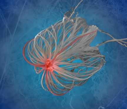 |
| With the help of laser beams material scientists from Saarbr³cken have made nanotubes grown on a silicium plate and have generated structures that look under the scanning electron microscope as a jellyfish in the sea. For this picture, the researchers received the highest award in the nationwide photography competition "Nano sichtbar machen", which means "Make Nano visible". Picture: "Nicolas Souza/cc-NanoBioNet e.V." |
Abstract:
Considered by some to be the "magic bullet" of materials science, carbon nanotubes (CNT) are at the forefront of materials research around the world. Carbon nanotubes are not only extremely stable, they are also excellent conductors of electrical energy and are made from a cheap raw material. Researchers at Saarland University want to use these highly versatile materials to help replace expensive precious metals in electrical contacts by cheaper alternatives such as nickel. By coating these replacement metals with nanotubes they hope to be able to prevent oxidation of the metal surface and thus avoid any associated reduction in electrical conductivity. By using lasers to help grow nanotubes on a silicon plate, the researchers in Saarbr³cken have created structures that, when viewed under a scanning electron microscope, resemble a jellyfish in the ocean. This image was recently awarded first prize in the national photo competition "Making Nano Visible".
Saarbr³cken material scientist wins national competition for best nanotechnology photo
Saarbr³cken, Germany | Posted on October 5th, 2011The competition was initiated by the three nanotechnology networks NanoBioNet, ASeNT-D and CeNTech. The Ć1000 prize will be awarded today at the WING.DE nanotechnology conference organized by the Federal Ministry of Education and Research (BMBF) in Berlin.
Pencils contain graphite, and graphite consists of carbon atoms aligned in layers. When we use a pencil for writing, these carbon atoms get deposited layer by layer. Nanotubes are essentially two-dimensional arrays of carbon atoms that have been rolled up as you would roll up a sheet of paper. "The result is tubes with a diameter of only ten nanometres, that is some 5000 times thinner than a human hair.
These nanotubes are extremely stable and are also excellent conductors of electrical energy," explains Nicolas Souza, doctoral student at the Department of Functional Materials headed by Professor Frank M³cklich. The challenge at present is to grow these nanotubes in a controlled way, such as depositing them as a lawn-like structure with the nanotubes attached to a contact surface. "We take a carbon mixture and by firing a laser at it we can raise the temperature of the target to about 6000░ causing it to vaporize at that point. The vaporized carbon atoms deposit on a nickel-coated silicon plate located below and grow to form nanotubes that rise up from the plate. The nickel merely acts as a catalyst and is not consumed in the process. Viewed under a scanning electron microscope, the final product has the appearance of a jellyfish containing a red nickel core," says Souza. His aim now is to try and establish even greater control over the growth process.
The Saarbr³cken researchers want to use the carbon nanotubes to replace the precious metals used in electrical contacts by cheaper alternatives such as nickel or copper. Up until now the problem has been that these metals tend to oxidize rapidly. Oxidation causes a deterioration in their surface properties and causes a significant reduction in their electrical conductivity. "If we can get the nanotubes to completely cover the surface of the metal then the nanotubes will act like the bristles of an upturned brush and will be able to penetrate the oxidation layer. This would give us improved electrical contact and the contact would be significantly more stable and more conductive than those produced by conventional means," explains Frank M³cklich, materials scientist at Saarland University and Director of the Steinbeis Material Engineering Center Saarland (MECS). This kind of technique would allow solar collectors to be designed much more efficiently or could enable the production of new products such as ultrathin and flexible computer screens.
In their search for new materials, the researchers in Professor M³cklich's team make use of a variety of laser techniques and 3D visualisation procedures, such as nanotomography. The Department of Functional Materials also recently took delivery of an atomic probe with which materials can be examined at the atomic scale and the results imaged in three dimensions.
####
For more information, please click here
Contacts:
Gordon Bolduan
Copyright © AlphaGalileo
If you have a comment, please Contact us.Issuers of news releases, not 7th Wave, Inc. or Nanotechnology Now, are solely responsible for the accuracy of the content.
Bookmark:


| Related News Press |
News and information
![]() Simulating magnetization in a Heisenberg quantum spin chain April 5th, 2024
Simulating magnetization in a Heisenberg quantum spin chain April 5th, 2024
![]() NRL charters NavyÆs quantum inertial navigation path to reduce drift April 5th, 2024
NRL charters NavyÆs quantum inertial navigation path to reduce drift April 5th, 2024
![]() Discovery points path to flash-like memory for storing qubits: Rice find could hasten development of nonvolatile quantum memory April 5th, 2024
Discovery points path to flash-like memory for storing qubits: Rice find could hasten development of nonvolatile quantum memory April 5th, 2024
Nanotubes/Buckyballs/Fullerenes/Nanorods/Nanostrings
![]() Tests find no free-standing nanotubes released from tire tread wear September 8th, 2023
Tests find no free-standing nanotubes released from tire tread wear September 8th, 2023
![]() Detection of bacteria and viruses with fluorescent nanotubes July 21st, 2023
Detection of bacteria and viruses with fluorescent nanotubes July 21st, 2023
Announcements
![]() NRL charters NavyÆs quantum inertial navigation path to reduce drift April 5th, 2024
NRL charters NavyÆs quantum inertial navigation path to reduce drift April 5th, 2024
![]() Discovery points path to flash-like memory for storing qubits: Rice find could hasten development of nonvolatile quantum memory April 5th, 2024
Discovery points path to flash-like memory for storing qubits: Rice find could hasten development of nonvolatile quantum memory April 5th, 2024
Human Interest/Art
![]() Drawing data in nanometer scale September 30th, 2022
Drawing data in nanometer scale September 30th, 2022
![]() Scientists prepare for the worldÆs smallest race: Nanocar Race II March 18th, 2022
Scientists prepare for the worldÆs smallest race: Nanocar Race II March 18th, 2022
![]() Graphene nanotubes revolutionize touch screen use for prosthetic hands August 3rd, 2021
Graphene nanotubes revolutionize touch screen use for prosthetic hands August 3rd, 2021
![]() JEOL Announces 2020 Microscopy Image Grand Prize Winners January 7th, 2021
JEOL Announces 2020 Microscopy Image Grand Prize Winners January 7th, 2021
Grants/Sponsored Research/Awards/Scholarships/Gifts/Contests/Honors/Records
![]() Discovery points path to flash-like memory for storing qubits: Rice find could hasten development of nonvolatile quantum memory April 5th, 2024
Discovery points path to flash-like memory for storing qubits: Rice find could hasten development of nonvolatile quantum memory April 5th, 2024
![]() Chemical reactions can scramble quantum information as well as black holes April 5th, 2024
Chemical reactions can scramble quantum information as well as black holes April 5th, 2024
|
|
||
|
|
||
| The latest news from around the world, FREE | ||
|
|
||
|
|
||
| Premium Products | ||
|
|
||
|
Only the news you want to read!
Learn More |
||
|
|
||
|
Full-service, expert consulting
Learn More |
||
|
|
||