Home > Press > Clemson, Hitachi unveil state-of-the-art electron microscope
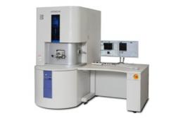 |
| The Hitachi NB5000 electron microscope image by: Hitachi |
Abstract:
Clemson University's Advanced Materials Research Laboratory (AMRL) now has one of the world's most-advanced electron microscopes that will further the university's leadership in nanotechnology and materials research.
Clemson, Hitachi unveil state-of-the-art electron microscope
Anderson, SC | Posted on October 4th, 2011Thanks to a strong partnership, Hitachi High Technologies America Inc., chose Clemson for the first university installation of the Hitachi NanoDuet NB5000 Focused Ion and Electron Beam System.
The electron microscope enhances the laboratory's ability to conduct research and advanced sample preparation for industry partners and academia, and affords Hitachi another location in which to showcase its products to the public and private sectors.
Clemson University President James F. Barker said the arrival of the microscope means the university can offer industry partners the latest nanotechnology innovation.
Clemson University and Hitachi have a successful history of collaboration.
"The relationship already has helped Clemson build what we believe is the nation's finest university-based electron microscope facility," Barker said. "Electron microscopy is one of the cornerstone research capabilities that is helping Clemson University drive innovation and economic development for our state and nation."
The ability to offer private companies the chance to examine and analyze materials for research and development on such sophisticated equipment means the university and Hitachi can forge working relationships with a wide array of sectors, he said.
JoAn Hudson, senior scientist and director of Clemson University's Electron Microscopy Facility, said focused ion beam systems first were used in the semiconductor industry, but the systems were too expensive for most academic institutions.
The microscope will allow researchers to work with "difficult" materials, such as thin film coatings: coatings that are 2 to 5 nanometers thick.
Other applications are the measurement of crack growth and aspect ratio during stress corrosion cracking and the study of adhesion properties of polymer coatings and the deformation of metal composites.
"We often take our surroundings for granted, but all of these examples affect our daily lives," Hudson said.
The electron microscope was formally unveiled Monday at a ceremony at the AMRL. Barker was joined by Craig Kerkove, executive vice president of Hitachi HTA; Toshihide Agemura, senior design engineer for NB5000 Hitachi; and other Clemson officials.
Hitachi's Kerkove said, "This collaboration between Clemson and Hitachi will certainly be one of the great events in Hitachi's 100-year history and will further our goal to not only be a manufacturer of scientific instruments, but to be an active partner with the academic community."
####
For more information, please click here
Contacts:
864-656-3311
Clemson University
Clemson, SC 29634
Copyright © Clemson University
If you have a comment, please Contact us.Issuers of news releases, not 7th Wave, Inc. or Nanotechnology Now, are solely responsible for the accuracy of the content.
Bookmark:


| Related News Press |
News and information
![]() Simulating magnetization in a Heisenberg quantum spin chain April 5th, 2024
Simulating magnetization in a Heisenberg quantum spin chain April 5th, 2024
![]() NRL charters Navy�s quantum inertial navigation path to reduce drift April 5th, 2024
NRL charters Navy�s quantum inertial navigation path to reduce drift April 5th, 2024
![]() Discovery points path to flash-like memory for storing qubits: Rice find could hasten development of nonvolatile quantum memory April 5th, 2024
Discovery points path to flash-like memory for storing qubits: Rice find could hasten development of nonvolatile quantum memory April 5th, 2024
Imaging
![]() Nanoscale CL thermometry with lanthanide-doped heavy-metal oxide in TEM March 8th, 2024
Nanoscale CL thermometry with lanthanide-doped heavy-metal oxide in TEM March 8th, 2024
![]() The USTC realizes In situ electron paramagnetic resonance spectroscopy using single nanodiamond sensors November 3rd, 2023
The USTC realizes In situ electron paramagnetic resonance spectroscopy using single nanodiamond sensors November 3rd, 2023
![]() Observation of left and right at nanoscale with optical force October 6th, 2023
Observation of left and right at nanoscale with optical force October 6th, 2023
Academic/Education
![]() Rice University launches Rice Synthetic Biology Institute to improve lives January 12th, 2024
Rice University launches Rice Synthetic Biology Institute to improve lives January 12th, 2024
![]() Multi-institution, $4.6 million NSF grant to fund nanotechnology training September 9th, 2022
Multi-institution, $4.6 million NSF grant to fund nanotechnology training September 9th, 2022
Announcements
![]() NRL charters Navy�s quantum inertial navigation path to reduce drift April 5th, 2024
NRL charters Navy�s quantum inertial navigation path to reduce drift April 5th, 2024
![]() Discovery points path to flash-like memory for storing qubits: Rice find could hasten development of nonvolatile quantum memory April 5th, 2024
Discovery points path to flash-like memory for storing qubits: Rice find could hasten development of nonvolatile quantum memory April 5th, 2024
Tools
![]() Ferroelectrically modulate the Fermi level of graphene oxide to enhance SERS response November 3rd, 2023
Ferroelectrically modulate the Fermi level of graphene oxide to enhance SERS response November 3rd, 2023
![]() The USTC realizes In situ electron paramagnetic resonance spectroscopy using single nanodiamond sensors November 3rd, 2023
The USTC realizes In situ electron paramagnetic resonance spectroscopy using single nanodiamond sensors November 3rd, 2023
|
|
||
|
|
||
| The latest news from around the world, FREE | ||
|
|
||
|
|
||
| Premium Products | ||
|
|
||
|
Only the news you want to read!
Learn More |
||
|
|
||
|
Full-service, expert consulting
Learn More |
||
|
|
||