Home > Press > NIST Polishes Method for Creating Tiny Diamond Machines
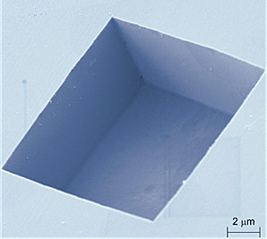 |
| This colorized electron microscope image reveals the boxy shape of the pits the NIST team etched into the diamond surface, exhibiting their smooth vertical sidewalls and flat bottom. The pits were between 1 and 72 micrometers in size.
Credit: NIST |
Abstract:
Diamonds may be best known as a symbol of long-lasting love. But semiconductor makers are also hoping they'll pan out as key components of long-lasting micromachines if a new method developed at the National Institute of Standards and Technology (NIST) for carving these tough, capable crystals proves its worth.* The method offers a precise way to engineer microscopic cuts in a diamond surface, yielding potential benefits in both measurement and technological fields.
NIST Polishes Method for Creating Tiny Diamond Machines
Gaithersburg, MD | Posted on September 30th, 2011By combining their own observations with background gleaned from materials science, NIST semiconductor researchers have found a way to create unique features in diamond�potentially leading to improvements in nanometrology in short order, as it has allowed the team to make holes of precise shape in one of the hardest known substances. But beyond the creation of virtually indestructible nanorulers, the method could one day lead to the improvement of a class of electronic devices useful in cell phones, gyroscopes and medical implants.
Well known for making the hugely complex electronic microchips that run our laptops, the semiconductor industry has expanded its portfolio by fabricating tiny devices with moving parts. Constructed with substantially the same techniques as the electronic chips, these "micro-electromechanical systems," or MEMS, are just a few micrometers in size. They can detect environmental changes such as heat, pressure and acceleration, potentially enabling them to form the basis of tiny sensors and actuators for a host of new devices. But designers must take care that tiny moving parts do not grind to a disastrous halt. One way to make the sliding parts last longer without breaking down is to make them from a tougher material than silicon.
"Diamond may be the ideal substance for MEMS devices," says NIST's Craig McGray. "It can withstand extreme conditions, plus it's able to vibrate at the very high frequencies that new consumer electronics demand. But it's very hard, of course, and there hasn't been a way to engineer it very precisely at small scales. We think our method can accomplish that."
The method uses a chemical etching process to create cavities in the diamond surface. The cubic shape of a diamond crystal can be sliced in several ways�a fact jewelers take advantage of when creating facets on gemstones. The speed of the etching process depends on the orientation of the slice, occurring at a far slower rate in the direction of the cube's "faces"�think of chopping the cube into smaller cubes�and these face planes can be used as a sort of boundary where etching can be made to stop when desired. In their initial experiments, the team created cavities ranging in width from 1 to 72 micrometers, each with smooth vertical sidewalls and a flat bottom.
"We'd like to figure out how to optimize control of this process next," McGray says, "but some of the ways diamond behaved under the conditions we used were unexpected. We plan to explore some of these mysteries while we develop a prototype diamond MEMS device."
* C.D. McGray, R.A. Allen, M. Cangemi and J. Geist. Rectangular scale-similar etch pits in monocrystalline diamond. Diamond and Related Materials. Available online 22 August 2011, ISSN 0925-9635, 10.1016/j.diamond.2011.08.007.
####
For more information, please click here
Contacts:
Chad Boutin
(301) 975-4261
Copyright © NIST
If you have a comment, please Contact us.Issuers of news releases, not 7th Wave, Inc. or Nanotechnology Now, are solely responsible for the accuracy of the content.
Bookmark:


| Related News Press |
News and information
![]() Simulating magnetization in a Heisenberg quantum spin chain April 5th, 2024
Simulating magnetization in a Heisenberg quantum spin chain April 5th, 2024
![]() NRL charters Navy�s quantum inertial navigation path to reduce drift April 5th, 2024
NRL charters Navy�s quantum inertial navigation path to reduce drift April 5th, 2024
![]() Discovery points path to flash-like memory for storing qubits: Rice find could hasten development of nonvolatile quantum memory April 5th, 2024
Discovery points path to flash-like memory for storing qubits: Rice find could hasten development of nonvolatile quantum memory April 5th, 2024
Laboratories
![]() A battery�s hopping ions remember where they�ve been: Seen in atomic detail, the seemingly smooth flow of ions through a battery�s electrolyte is surprisingly complicated February 16th, 2024
A battery�s hopping ions remember where they�ve been: Seen in atomic detail, the seemingly smooth flow of ions through a battery�s electrolyte is surprisingly complicated February 16th, 2024
![]() NRL discovers two-dimensional waveguides February 16th, 2024
NRL discovers two-dimensional waveguides February 16th, 2024
![]() Three-pronged approach discerns qualities of quantum spin liquids November 17th, 2023
Three-pronged approach discerns qualities of quantum spin liquids November 17th, 2023
Govt.-Legislation/Regulation/Funding/Policy
![]() NRL charters Navy�s quantum inertial navigation path to reduce drift April 5th, 2024
NRL charters Navy�s quantum inertial navigation path to reduce drift April 5th, 2024
![]() Discovery points path to flash-like memory for storing qubits: Rice find could hasten development of nonvolatile quantum memory April 5th, 2024
Discovery points path to flash-like memory for storing qubits: Rice find could hasten development of nonvolatile quantum memory April 5th, 2024
![]() Chemical reactions can scramble quantum information as well as black holes April 5th, 2024
Chemical reactions can scramble quantum information as well as black holes April 5th, 2024
MEMS
Chip Technology
![]() Discovery points path to flash-like memory for storing qubits: Rice find could hasten development of nonvolatile quantum memory April 5th, 2024
Discovery points path to flash-like memory for storing qubits: Rice find could hasten development of nonvolatile quantum memory April 5th, 2024
![]() Utilizing palladium for addressing contact issues of buried oxide thin film transistors April 5th, 2024
Utilizing palladium for addressing contact issues of buried oxide thin film transistors April 5th, 2024
![]() HKUST researchers develop new integration technique for efficient coupling of III-V and silicon February 16th, 2024
HKUST researchers develop new integration technique for efficient coupling of III-V and silicon February 16th, 2024
Nanomedicine
![]() New micromaterial releases nanoparticles that selectively destroy cancer cells April 5th, 2024
New micromaterial releases nanoparticles that selectively destroy cancer cells April 5th, 2024
![]() Good as gold - improving infectious disease testing with gold nanoparticles April 5th, 2024
Good as gold - improving infectious disease testing with gold nanoparticles April 5th, 2024
![]() Researchers develop artificial building blocks of life March 8th, 2024
Researchers develop artificial building blocks of life March 8th, 2024
Sensors
Discoveries
![]() Chemical reactions can scramble quantum information as well as black holes April 5th, 2024
Chemical reactions can scramble quantum information as well as black holes April 5th, 2024
![]() New micromaterial releases nanoparticles that selectively destroy cancer cells April 5th, 2024
New micromaterial releases nanoparticles that selectively destroy cancer cells April 5th, 2024
![]() Utilizing palladium for addressing contact issues of buried oxide thin film transistors April 5th, 2024
Utilizing palladium for addressing contact issues of buried oxide thin film transistors April 5th, 2024
Materials/Metamaterials/Magnetoresistance
![]() Nanoscale CL thermometry with lanthanide-doped heavy-metal oxide in TEM March 8th, 2024
Nanoscale CL thermometry with lanthanide-doped heavy-metal oxide in TEM March 8th, 2024
![]() Focused ion beam technology: A single tool for a wide range of applications January 12th, 2024
Focused ion beam technology: A single tool for a wide range of applications January 12th, 2024
Announcements
![]() NRL charters Navy�s quantum inertial navigation path to reduce drift April 5th, 2024
NRL charters Navy�s quantum inertial navigation path to reduce drift April 5th, 2024
![]() Discovery points path to flash-like memory for storing qubits: Rice find could hasten development of nonvolatile quantum memory April 5th, 2024
Discovery points path to flash-like memory for storing qubits: Rice find could hasten development of nonvolatile quantum memory April 5th, 2024
|
|
||
|
|
||
| The latest news from around the world, FREE | ||
|
|
||
|
|
||
| Premium Products | ||
|
|
||
|
Only the news you want to read!
Learn More |
||
|
|
||
|
Full-service, expert consulting
Learn More |
||
|
|
||