Home > Press > Biological Interface Using Piezotronics: Resistive Switches Based on Piezoelectric Nanowires Allow Electrical Signals to be Produced from Mechanical Actions
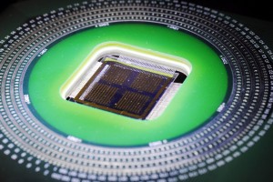 |
| An array of piezoelectrically modulated resistive memory (PRM) cells is shown being studied in an optical microscope. Credit: Gary Meek |
Abstract:
Taking advantage of the unique properties of zinc oxide nanowires, researchers have demonstrated a new type of piezoelectric resistive switching device in which the write-read access of memory cells is controlled by electromechanical modulation. Operating on flexible substrates, arrays of these devices could provide a new way to interface the mechanical actions of the biological world to conventional electronic circuitry.
Biological Interface Using Piezotronics: Resistive Switches Based on Piezoelectric Nanowires Allow Electrical Signals to be Produced from Mechanical Actions
Atlanta, GA | Posted on July 26th, 2011The piezoelectrically modulated resistive memory (PRM) devices take advantage of the fact that the resistance of piezoelectric semiconducting materials such as zinc oxide (ZnO) can be controlled through the application of strain from a mechanical action. The change in resistance can be detected electronically, providing a simple way to obtain an electronic signal from a mechanical action.
"We can provide the interface between biology and electronics," said Zhong Lin Wang, Regents professor in the School of Materials Science and Engineering at the Georgia Institute of Technology. "This technology, which is based on zinc oxide nanowires, allows communication between a mechanical action in the biological world and conventional devices in the electronic world."
The research was reported online June 22 in the journal Nano Letters. The work was sponsored by the Defense Advanced Research Projects Agency (DARPA), the National Science Foundation (NSF), the U.S. Air Force and the U.S. Department of Energy.
In conventional transistors, the flow of current between a source and a drain is controlled by a gate voltage applied to the device. That gate voltage determines whether the device is on or off.
The piezotronic memory devices developed by Wang and graduate student Wenzhuo Wu take advantage of the fact that piezoelectric materials like zinc oxide produce a charge potential when they are mechanically deformed or otherwise put under strain. These PRM devices use the piezoelectric charge created by the deformation to control the current flowing through the zinc oxide nanowires that are at the heart of the devices - the basic principle of piezotronics. The charge creates polarity in the nanowires - and increases the electrical resistance much like gate voltage in a conventional transistor.
"We are replacing the application of an external voltage with the production of an internal voltage," Wang explained. "Because zinc oxide is both piezoelectric and semiconducting, when you strain the material with a mechanical action, you create a piezopotential. This piezopotential tunes the charge transport across the interface - instead of controlling channel width as in conventional field effect transistors."
The mechanical strain could come from mechanical activities as diverse as signing a name with a pen, the motion of an actuator on a nanorobot, or biological activities of the human body such as a heart beating.
"We control the charge flow across the interface using strain," Wang explained. "If you have no strain, the charge flows normally. But if you apply a strain, the resulting voltage builds a barrier that controls the flow."
The piezotronic switching affects current flowing in just one direction, depending whether the strain is tensile or compressive. That means the memory stored in the piezotronic devices has both a sign and a magnitude. The information in this memory can be read, processed and stored through conventional electronic means.
Taking advantage of large-scale fabrication techniques for zinc oxide nanowire arrays, the Georgia Tech researchers have built non-volatile resistive switching memories for use as a storage medium. They have shown that these piezotronic devices can be written, that information can be read from them, and that they can be erased for re-use. About 20 of the arrays have been built so far for testing.
The zinc oxide nanowires, which are about 500 nanometers in diameter and about 50 microns long, are produced with a physical vapor deposition process that uses a high-temperature furnace. The resulting structures are then treated with oxygen plasma to reduce the number of crystalline defects - which helps to control their conductivity. The arrays are then transferred to a flexible substrate.
"The switching voltage is tunable, depending on the number of oxygen vacancies in the structure," Wang said. "The more defects you quench away with the oxygen plasma, the larger the voltage that will be required to drive current flow."
The piezotronic memory cells operate at low frequencies, which are appropriate for the kind of biologically-generated signals they will record, Wang said.
These piezotronic memory elements provide another component needed for fabricating complete self-powered nanoelectromechanical systems (NEMS) on a single chip. Wang's research team has already demonstrated other key elements such as nanogenerators, sensors and wireless transmitters.
"We are taking another step toward the goal of self-powered complete systems," Wang said. "The challenges now are to make them small enough to be integrated onto a single chip. We believe these systems will solve important problems in people's lives."
Wang believes this new memory will become increasingly important as devices become more closely connected to individual human activities. The ability to build these devices on flexible substrates means they can be used in the body - and with other electronic devices now being built on materials that are not traditional silicon.
"As computers and other electronic devices become more personalized and human-like, we will need to develop new types of signals, interfacing mechanical actions to electronics," he said. "Piezoelectric materials provide the most sensitive way to translate these gentle mechanical actions into electronic signals that can be used by electronic devices."
####
For more information, please click here
Contacts:
John Toon, Manager
Research News & Publications Office
Georgia Institute of Technology
75 Fifth Street, N.W., Suite 314
Atlanta, Georgia 30308 USA
Phone: 404-894-6986
Web: gtresearchnews.gatech.edu
Twitter: @gtresearchnews
Abby Robinson
404-385-3364
Copyright © Georgia Institute of Technology
If you have a comment, please Contact us.Issuers of news releases, not 7th Wave, Inc. or Nanotechnology Now, are solely responsible for the accuracy of the content.
Bookmark:


| Related News Press |
News and information
![]() Simulating magnetization in a Heisenberg quantum spin chain April 5th, 2024
Simulating magnetization in a Heisenberg quantum spin chain April 5th, 2024
![]() NRL charters Navy�s quantum inertial navigation path to reduce drift April 5th, 2024
NRL charters Navy�s quantum inertial navigation path to reduce drift April 5th, 2024
![]() Discovery points path to flash-like memory for storing qubits: Rice find could hasten development of nonvolatile quantum memory April 5th, 2024
Discovery points path to flash-like memory for storing qubits: Rice find could hasten development of nonvolatile quantum memory April 5th, 2024
Chip Technology
![]() Discovery points path to flash-like memory for storing qubits: Rice find could hasten development of nonvolatile quantum memory April 5th, 2024
Discovery points path to flash-like memory for storing qubits: Rice find could hasten development of nonvolatile quantum memory April 5th, 2024
![]() Utilizing palladium for addressing contact issues of buried oxide thin film transistors April 5th, 2024
Utilizing palladium for addressing contact issues of buried oxide thin film transistors April 5th, 2024
![]() HKUST researchers develop new integration technique for efficient coupling of III-V and silicon February 16th, 2024
HKUST researchers develop new integration technique for efficient coupling of III-V and silicon February 16th, 2024
Memory Technology
![]() Utilizing palladium for addressing contact issues of buried oxide thin film transistors April 5th, 2024
Utilizing palladium for addressing contact issues of buried oxide thin film transistors April 5th, 2024
![]() Interdisciplinary: Rice team tackles the future of semiconductors Multiferroics could be the key to ultralow-energy computing October 6th, 2023
Interdisciplinary: Rice team tackles the future of semiconductors Multiferroics could be the key to ultralow-energy computing October 6th, 2023
![]() Researchers discover materials exhibiting huge magnetoresistance June 9th, 2023
Researchers discover materials exhibiting huge magnetoresistance June 9th, 2023
Nanoelectronics
![]() Interdisciplinary: Rice team tackles the future of semiconductors Multiferroics could be the key to ultralow-energy computing October 6th, 2023
Interdisciplinary: Rice team tackles the future of semiconductors Multiferroics could be the key to ultralow-energy computing October 6th, 2023
![]() Key element for a scalable quantum computer: Physicists from Forschungszentrum J�lich and RWTH Aachen University demonstrate electron transport on a quantum chip September 23rd, 2022
Key element for a scalable quantum computer: Physicists from Forschungszentrum J�lich and RWTH Aachen University demonstrate electron transport on a quantum chip September 23rd, 2022
![]() Reduced power consumption in semiconductor devices September 23rd, 2022
Reduced power consumption in semiconductor devices September 23rd, 2022
![]() Atomic level deposition to extend Moore�s law and beyond July 15th, 2022
Atomic level deposition to extend Moore�s law and beyond July 15th, 2022
Discoveries
![]() Chemical reactions can scramble quantum information as well as black holes April 5th, 2024
Chemical reactions can scramble quantum information as well as black holes April 5th, 2024
![]() New micromaterial releases nanoparticles that selectively destroy cancer cells April 5th, 2024
New micromaterial releases nanoparticles that selectively destroy cancer cells April 5th, 2024
![]() Utilizing palladium for addressing contact issues of buried oxide thin film transistors April 5th, 2024
Utilizing palladium for addressing contact issues of buried oxide thin film transistors April 5th, 2024
Announcements
![]() NRL charters Navy�s quantum inertial navigation path to reduce drift April 5th, 2024
NRL charters Navy�s quantum inertial navigation path to reduce drift April 5th, 2024
![]() Discovery points path to flash-like memory for storing qubits: Rice find could hasten development of nonvolatile quantum memory April 5th, 2024
Discovery points path to flash-like memory for storing qubits: Rice find could hasten development of nonvolatile quantum memory April 5th, 2024
Battery Technology/Capacitors/Generators/Piezoelectrics/Thermoelectrics/Energy storage
![]() What heat can tell us about battery chemistry: using the Peltier effect to study lithium-ion cells March 8th, 2024
What heat can tell us about battery chemistry: using the Peltier effect to study lithium-ion cells March 8th, 2024
![]() A battery�s hopping ions remember where they�ve been: Seen in atomic detail, the seemingly smooth flow of ions through a battery�s electrolyte is surprisingly complicated February 16th, 2024
A battery�s hopping ions remember where they�ve been: Seen in atomic detail, the seemingly smooth flow of ions through a battery�s electrolyte is surprisingly complicated February 16th, 2024
Nanobiotechnology
![]() New micromaterial releases nanoparticles that selectively destroy cancer cells April 5th, 2024
New micromaterial releases nanoparticles that selectively destroy cancer cells April 5th, 2024
![]() Good as gold - improving infectious disease testing with gold nanoparticles April 5th, 2024
Good as gold - improving infectious disease testing with gold nanoparticles April 5th, 2024
![]() Researchers develop artificial building blocks of life March 8th, 2024
Researchers develop artificial building blocks of life March 8th, 2024
|
|
||
|
|
||
| The latest news from around the world, FREE | ||
|
|
||
|
|
||
| Premium Products | ||
|
|
||
|
Only the news you want to read!
Learn More |
||
|
|
||
|
Full-service, expert consulting
Learn More |
||
|
|
||