Home > Press > Hot AFM Draws Ferroelectric Nanostructures on Plastic
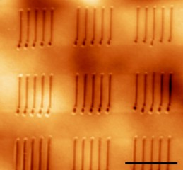 |
| (Courtesy Suenne Kim)
Image shows the topography (by atomic force microscope) of a ferroelectric PTO line array crystallized on a 360-nanometer thick precursor film on polyimide. The scale bar corresponds to one micron. |
Abstract:
Using a technique known as thermochemical nanolithography (TCNL), researchers have developed a new way to fabricate nanometer-scale ferroelectric structures directly on flexible plastic substrates that would be unable to withstand the processing temperatures normally required to create such nanostructures.
Hot AFM Draws Ferroelectric Nanostructures on Plastic
Atlanta, GA | Posted on July 18th, 2011The technique, which uses a heated atomic force microscope (AFM) tip to produce patterns, could facilitate high-density, low-cost production of complex ferroelectric structures for energy harvesting arrays, sensors and actuators in nano-electromechanical systems (NEMS) and micro-electromechanical systems (MEMS). The research was reported July 15 in the journal Advanced Materials.
"We can directly create piezoelectric materials of the shape we want, where we want them, on flexible substrates for use in energy harvesting and other applications," said Nazanin Bassiri-Gharb, co-author of the paper and an assistant professor in the School of Mechanical Engineering at the Georgia Institute of Technology. "This is the first time that structures like these have been directly grown with a CMOS-compatible process at such a small resolution. Not only have we been able to grow these ferroelectric structures at low substrate temperatures, but we have also been able to pattern them at very small scales."
The research was sponsored by the National Science Foundation and the U.S. Department of Energy. In addition to the Georgia Tech researchers, the work also involved scientists from the University of Illinois Urbana-Champaign and the University of Nebraska Lincoln.
The researchers have produced wires approximately 30 nanometers wide and spheres with diameters of approximately 10 nanometers using the patterning technique. Spheres with potential application as ferroelectric memory were fabricated at densities exceeding 200 gigabytes per square inch - currently the record for this perovskite-type ferroelectric material, said Suenne Kim, the paper's first author and a postdoctoral fellow in laboratory of Professor Elisa Riedo in Georgia Tech's School of Physics.
Ferroelectric materials are attractive because they exhibit charge-generating piezoelectric responses an order of magnitude larger than those of materials such as aluminum nitride or zinc oxide. The polarization of the materials can be easily and rapidly changed, giving them potential application as random access memory elements.
But the materials can be difficult to fabricate, requiring temperatures greater than 600 degrees Celsius for crystallization. Chemical etching techniques produce grain sizes as large as the nanoscale features researchers would like to produce, while physical etching processes damage the structures and reduce their attractive properties. Until now, these challenges required that ferroelectric structures be grown on a single-crystal substrate compatible with high temperatures, then transferred to a flexible substrate for use in energy-harvesting.
The thermochemical nanolithography process, which was developed at Georgia Tech in 2007, addresses those challenges by using extremely localized heating to form structures only where the resistively-heated AFM tip contacts a precursor material. A computer controls the AFM writing, allowing the researchers to create patterns of crystallized material where desired. To create energy-harvesting structures, for example, lines corresponding to ferroelectric nanowires can be drawn along the direction in which strain would be applied.
"The heat from the AFM tip crystallizes the amorphous precursor to make the structure," Bassiri-Gharb explained. "The patterns are formed only where the crystallization occurs."
To begin the fabrication, the sol-gel precursor material is first applied to a substrate with a standard spin-coating method, then briefly heated to approximately 250 degrees Celsius to drive off the organic solvents. The researchers have used polyimide, glass and silicon substrates, but in principle, any material able to withstand the 250-degree heating step could be used. Structures have been made from Pb(ZrTi)O3 - known as PZT, and PbTiO3 - known as PTO.
"We still heat the precursor at the temperatures required to crystallize the structure, but the heating is so localized that it does not affect the substrate," explained Riedo, a co-author of the paper and an associate professor in the Georgia Tech School of Physics.
The heated AFM tips were provided by William King, a professor in the Department of Mechanical Science and Engineering at the University of Illinois at Urbana-Champaign.
As a next step, the researchers plan to use arrays of AFM tips to produce larger patterned areas, and improve the heated AFM tips to operate for longer periods of time. The researchers also hope to understand the basic science behind ferroelectric materials, including properties at the nanoscale.
"We need to look at the growth thermodynamics of these ferroelectric materials," said Bassiri-Gharb. "We also need to see how the properties change when you move from the bulk to the micron scale and then to the nanometer scale. We need to understand what really happens to the extrinsic and intrinsic responses of the materials at these small scales."
Ultimately, arrays of AFM tips under computer control could produce complete devices, providing an alternative to current fabrication techniques.
"Thermochemical nanolithography is a very powerful nanofabrication technique that, through heating, is like a nanoscale pen that can create nanostructures useful in a variety of applications, including protein arrays, DNA arrays, and graphene-like nanowires," Riedo explained. "We are really addressing the problem caused by the existing limitations of photolithography at these size scales. We can envision creating a full device based on the same fabrication technique without the requirements of costly clean rooms and vacuum-based equipment. We are moving toward a process in which multiple steps are done using the same tool to pattern at the small scale."
In addition to those already mentioned, the research team included Yaser Bastani from the G.W. Woodruff School of Mechanical Engineering at Georgia Tech, Seth Marder and Kenneth Sandhage, both from Georgia Tech's School of Chemistry and Biochemistry and School of Materials Science and Engineering, and Alexei Gruverman and Haidong Lu from the Department of Physics and Astronomy at the University of Nebraska-Lincoln.
####
For more information, please click here
Contacts:
Research News & Publications Office
Georgia Institute of Technology
75 Fifth Street, N.W., Suite 314
Atlanta, Georgia 30308 USA
John Toon
404-894-6986
or
Abby Robinson
404-385-3364
Copyright © Newswise
If you have a comment, please Contact us.Issuers of news releases, not 7th Wave, Inc. or Nanotechnology Now, are solely responsible for the accuracy of the content.
Bookmark:


| Related News Press |
News and information
![]() Simulating magnetization in a Heisenberg quantum spin chain April 5th, 2024
Simulating magnetization in a Heisenberg quantum spin chain April 5th, 2024
![]() NRL charters Navy�s quantum inertial navigation path to reduce drift April 5th, 2024
NRL charters Navy�s quantum inertial navigation path to reduce drift April 5th, 2024
![]() Discovery points path to flash-like memory for storing qubits: Rice find could hasten development of nonvolatile quantum memory April 5th, 2024
Discovery points path to flash-like memory for storing qubits: Rice find could hasten development of nonvolatile quantum memory April 5th, 2024
Chip Technology
![]() Discovery points path to flash-like memory for storing qubits: Rice find could hasten development of nonvolatile quantum memory April 5th, 2024
Discovery points path to flash-like memory for storing qubits: Rice find could hasten development of nonvolatile quantum memory April 5th, 2024
![]() Utilizing palladium for addressing contact issues of buried oxide thin film transistors April 5th, 2024
Utilizing palladium for addressing contact issues of buried oxide thin film transistors April 5th, 2024
![]() HKUST researchers develop new integration technique for efficient coupling of III-V and silicon February 16th, 2024
HKUST researchers develop new integration technique for efficient coupling of III-V and silicon February 16th, 2024
Nanoelectronics
![]() Interdisciplinary: Rice team tackles the future of semiconductors Multiferroics could be the key to ultralow-energy computing October 6th, 2023
Interdisciplinary: Rice team tackles the future of semiconductors Multiferroics could be the key to ultralow-energy computing October 6th, 2023
![]() Key element for a scalable quantum computer: Physicists from Forschungszentrum J�lich and RWTH Aachen University demonstrate electron transport on a quantum chip September 23rd, 2022
Key element for a scalable quantum computer: Physicists from Forschungszentrum J�lich and RWTH Aachen University demonstrate electron transport on a quantum chip September 23rd, 2022
![]() Reduced power consumption in semiconductor devices September 23rd, 2022
Reduced power consumption in semiconductor devices September 23rd, 2022
![]() Atomic level deposition to extend Moore�s law and beyond July 15th, 2022
Atomic level deposition to extend Moore�s law and beyond July 15th, 2022
Discoveries
![]() Chemical reactions can scramble quantum information as well as black holes April 5th, 2024
Chemical reactions can scramble quantum information as well as black holes April 5th, 2024
![]() New micromaterial releases nanoparticles that selectively destroy cancer cells April 5th, 2024
New micromaterial releases nanoparticles that selectively destroy cancer cells April 5th, 2024
![]() Utilizing palladium for addressing contact issues of buried oxide thin film transistors April 5th, 2024
Utilizing palladium for addressing contact issues of buried oxide thin film transistors April 5th, 2024
Announcements
![]() NRL charters Navy�s quantum inertial navigation path to reduce drift April 5th, 2024
NRL charters Navy�s quantum inertial navigation path to reduce drift April 5th, 2024
![]() Discovery points path to flash-like memory for storing qubits: Rice find could hasten development of nonvolatile quantum memory April 5th, 2024
Discovery points path to flash-like memory for storing qubits: Rice find could hasten development of nonvolatile quantum memory April 5th, 2024
Printing/Lithography/Inkjet/Inks/Bio-printing/Dyes
![]() Presenting: Ultrasound-based printing of 3D materials�potentially inside the body December 8th, 2023
Presenting: Ultrasound-based printing of 3D materials�potentially inside the body December 8th, 2023
![]() Simple ballpoint pen can write custom LEDs August 11th, 2023
Simple ballpoint pen can write custom LEDs August 11th, 2023
![]() Disposable electronics on a simple sheet of paper October 7th, 2022
Disposable electronics on a simple sheet of paper October 7th, 2022
|
|
||
|
|
||
| The latest news from around the world, FREE | ||
|
|
||
|
|
||
| Premium Products | ||
|
|
||
|
Only the news you want to read!
Learn More |
||
|
|
||
|
Full-service, expert consulting
Learn More |
||
|
|
||