Home > Press > Picosun and Carleton University Introduce the First Gold Films by Plasma-Enhanced ALD
 |
Abstract:
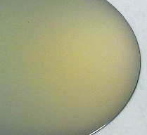
Picosun Oy, Finland-based global manufacturer of state-of-the-art Atomic Layer Deposition (ALD) equipment, reports successful process for preparation of gold thin films with plasma-enhanced ALD (PEALD) method first time in the world. Gold films were grown in Picosun's SUNALE˙ ALD reactor equipped with the same company‚s Picoplasma˙ plasma source system on top of ruthenium underlayers, as illustrated in the photograph below, from precursor chemicals developed and synthesized by Prof. Sean Barry and Ph.D. student Jason Coyle from Carleton University, Ottawa, Canada.
Picosun and Carleton University Introduce the First Gold Films by Plasma-Enhanced ALD
Espoo, Finland | Posted on July 11th, 2011Picosun has worked with precursor and process development with Carleton University also before. Copper films of excellent quality and uniformity have been deposited on top of TiN underlayers and on silicon trench wafers, on the bottom of trenches of aspect ratio 1:15. Moreover, high quality silver thin films have been successfully manufactured in a Picosun SUNALE˙ reactor from precursors developed at the University of Helsinki, Finland.
Production of ultra-thin, highly uniform and conformal metal films even on high aspect ratio structures such as Through-Silicon-Vias (TSV) and other 3D nanoscale architectures is becoming crucial in today's electronics manufacturing. As the component sizes keep decreasing but at the same time, the level of system integration increasing, metal deposition by ALD is the only method with which conductive layers and contact points can be manufactured on the nm-scale patterned, 3D-integrated, highly complex modern MEMS/NEMS (Micro/NanoElectroMechanical) devices.
"Coinage metals (Cu, Ag, Au) are poised to play a significant role also in sensing technologies, where they will be crucial in signal enhancement and as anchor surfaces for organic sensing elements. Using plasma to deposit these metals as an ALD process widens drastically the deposition temperature window, permitting the employment of such sensitive substrates as modified fiber optic filaments and plastics. The design of the Picoplasma˙ tool allows for excellent uniformity over a wide deposition area, while minimizing substrate damage from the plasma source", states Prof. Barry from Carleton University.
Picosun's Picoplasma˙, innovative and revolutionary "ion-free" remote plasma source was just recently launched to the market and it has been a huge success right from the start, being already chosen by several key customers on three continents.
####
About Picosun Oy
Picosun Oy is a Finland-based global manufacturer of state-of-the-art ALD systems for micro- and nanotechnology applications, representing continuity to over three decades of dedicated, exclusive ALD reactor design and manufacturing. Picosun is based in Espoo, Finland, its production facilities are located in Kirkkonummi, Finland, and its US headquarters in Detroit, Michigan. Picosun‚s SUNALE˙ ALD process tools are in daily use in various top level universities, research institutes and high profile companies across four continents. Picosun Oy is a part of Stephen Industries Inc. Oy.
For more information, please click here
Contacts:
Juhana Kostamo
Phone: +358 50 321 1955
Fax: +358 20 722 7012
E-mail:
Copyright © Picosun Oy
If you have a comment, please Contact us.Issuers of news releases, not 7th Wave, Inc. or Nanotechnology Now, are solely responsible for the accuracy of the content.
Bookmark:


| Related News Press |
News and information
![]() Simulating magnetization in a Heisenberg quantum spin chain April 5th, 2024
Simulating magnetization in a Heisenberg quantum spin chain April 5th, 2024
![]() NRL charters Navy’s quantum inertial navigation path to reduce drift April 5th, 2024
NRL charters Navy’s quantum inertial navigation path to reduce drift April 5th, 2024
![]() Discovery points path to flash-like memory for storing qubits: Rice find could hasten development of nonvolatile quantum memory April 5th, 2024
Discovery points path to flash-like memory for storing qubits: Rice find could hasten development of nonvolatile quantum memory April 5th, 2024
![]() Good as gold - improving infectious disease testing with gold nanoparticles April 5th, 2024
Good as gold - improving infectious disease testing with gold nanoparticles April 5th, 2024
Thin films
![]() Utilizing palladium for addressing contact issues of buried oxide thin film transistors April 5th, 2024
Utilizing palladium for addressing contact issues of buried oxide thin film transistors April 5th, 2024
![]() Understanding the mechanism of non-uniform formation of diamond film on tools: Paving the way to a dry process with less environmental impact March 24th, 2023
Understanding the mechanism of non-uniform formation of diamond film on tools: Paving the way to a dry process with less environmental impact March 24th, 2023
![]() New study introduces the best graphite films: The work by Distinguished Professor Feng Ding at UNIST has been published in the October 2022 issue of Nature Nanotechnology November 4th, 2022
New study introduces the best graphite films: The work by Distinguished Professor Feng Ding at UNIST has been published in the October 2022 issue of Nature Nanotechnology November 4th, 2022
NEMS
![]() IEDM - CEA-Leti Will Present 11 Papers and Host Workshop on Disruptive Technologies for Data Management November 7th, 2018
IEDM - CEA-Leti Will Present 11 Papers and Host Workshop on Disruptive Technologies for Data Management November 7th, 2018
![]() UT engineers develop first method for controlling nanomotors: Breakthrough for nanotechnology as UT engineers develop first method for switching the mechanical motion of nanomotors September 21st, 2018
UT engineers develop first method for controlling nanomotors: Breakthrough for nanotechnology as UT engineers develop first method for switching the mechanical motion of nanomotors September 21st, 2018
![]() Nano-kirigami: 'Paper-cut' provides model for 3D intelligent nanofabrication July 13th, 2018
Nano-kirigami: 'Paper-cut' provides model for 3D intelligent nanofabrication July 13th, 2018
![]() One string to rule them all April 17th, 2018
One string to rule them all April 17th, 2018
MEMS
Discoveries
![]() Chemical reactions can scramble quantum information as well as black holes April 5th, 2024
Chemical reactions can scramble quantum information as well as black holes April 5th, 2024
![]() New micromaterial releases nanoparticles that selectively destroy cancer cells April 5th, 2024
New micromaterial releases nanoparticles that selectively destroy cancer cells April 5th, 2024
![]() Utilizing palladium for addressing contact issues of buried oxide thin film transistors April 5th, 2024
Utilizing palladium for addressing contact issues of buried oxide thin film transistors April 5th, 2024
Announcements
![]() NRL charters Navy’s quantum inertial navigation path to reduce drift April 5th, 2024
NRL charters Navy’s quantum inertial navigation path to reduce drift April 5th, 2024
![]() Discovery points path to flash-like memory for storing qubits: Rice find could hasten development of nonvolatile quantum memory April 5th, 2024
Discovery points path to flash-like memory for storing qubits: Rice find could hasten development of nonvolatile quantum memory April 5th, 2024
Tools
![]() Ferroelectrically modulate the Fermi level of graphene oxide to enhance SERS response November 3rd, 2023
Ferroelectrically modulate the Fermi level of graphene oxide to enhance SERS response November 3rd, 2023
![]() The USTC realizes In situ electron paramagnetic resonance spectroscopy using single nanodiamond sensors November 3rd, 2023
The USTC realizes In situ electron paramagnetic resonance spectroscopy using single nanodiamond sensors November 3rd, 2023
|
|
||
|
|
||
| The latest news from around the world, FREE | ||
|
|
||
|
|
||
| Premium Products | ||
|
|
||
|
Only the news you want to read!
Learn More |
||
|
|
||
|
Full-service, expert consulting
Learn More |
||
|
|
||