Home > Press > Splitsville for Boron Nitride Nanotubes: Berkeley Lab Researchers Find New Way to Mass Produce High Quality Boron Nitride Nanoribbons
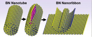 |
| Splitting of a boron nitride nanotube to form a boron nitride nanoribbon shows atoms of boron in blue, nitrogen in yellow and potassium in pink. Pressure from potassium intercalation unzips the BNNT and forms layers of BNNRs. |
Abstract:
For Hollywood celebrities, the term "splitsville" usually means "check your prenup." For scientists wanting to mass-produce high quality nanoribbons from boron nitride nanotubes, "splitsville" could mean "happily ever after."
Splitsville for Boron Nitride Nanotubes: Berkeley Lab Researchers Find New Way to Mass Produce High Quality Boron Nitride Nanoribbons
Berkeley, CA | Posted on July 2nd, 2011Scientists with the Lawrence Berkeley National Laboratory (Berkeley Lab) and the University of California (UC) Berkeley, working with scientists at Rice University, have developed a technique in which boron nitride nanotubes are stuffed with atoms of potassium until the tubes split open along a longitudinal seam. This creates defect-free boron nitride nanoribbons of uniform lengths and thickness. Boron nitride nanoribbons are projected to display a variety of intriguing magnetic and electronic properties that hold enormous potential for future devices.
Nanoribbons are two-dimensional single crystals (meaning only a single atom in thickness) that can measure multiple microns in length, but only a few hundred or less nanometers in width. Graphene nanoribbons, which are made from pure carbon, carry electrons at much faster speeds than silicon, and can be used to cover wide areas and a broad assortment of shapes. Boron nitride nanoribbons offer similar advantages plus an additional array of electronic, optical and magnetic properties.
"There has been a significant amount of theoretical work indicating that, depending on the ribbon edges, boron nitride nanoribbons may exhibit ferromagnetism or anti-ferromagnetism, as well as spin-polarized transport which is either metallic or semi-conducting," says physicist Alex Zettl, one of the world's foremost researchers into nanoscale systems and devices who holds joint appointments with Berkeley Lab's Materials Sciences Division (MSD) and the Physics Department at UC Berkeley, where he is the director of the Center of Integrated Nanomechanical Systems (COINS).
"The unique properties of boron nitride nanoribbons are of great fundamental scientific interest and also have implications for applications in technologies that include spintronics and optoelectronics," Zettl says. "However, the facile, scalable synthesis of high quality boron nitride nanoribbons has been a significant challenge."
Zettl and members of his research group met this challenge using the chemical process known as "intercalation," whereby atoms or molecules of one type are inserted between atoms and molecules of another type. James Tour at Rice University and his research group had demonstrated that the intercalation of potassium atoms into carbon nanotubes promotes a longitudinal splitting of the tubes. This prompted Zettl and Tour to collaborate on a study that used the same approach on boron nitride nanotubes, which are very similar in structure to nanotubes made from carbon.
Zettl and Tour reported the results of this study in the journal Nano Letters. The paper was titled "Longitudinal Splitting of Boron Nitride Nanotubes for the Facile Synthesis of High Quality Boron Nitride Nanoribbons." Co-authoring the paper were Kris Erickson, Ashley Gibb, Michael Rousseas and Nasim Alem, who are all members of Zettl's research group, and Alexander Sinitskii, a member of Tour's research group.
"The likely mechanism for the splitting of both carbon and boron nitride nanotubes is that potassium islands grow from an initial starting point of intercalation," Zettl says. "This island growth continues until enough circumferential strain results in a breakage of the chemical bonds of the intercalated nanotube. The potassium then begins bonding to the bare ribbon edge, inducing further splitting."
This synthesis technique yields boron nitride nanoribbons of uniform widths that can be as narrow as 20 nanometers. The ribbons are also at least one micron in length, with minimal defects within the plane or along the edges. Zettl says the high quality of the edges points to the splitting process being orderly rather than random. This orderliness could explain why a high proportion of the boron nitride nanoribbons display the coveted zigzag or armchair-shaped edges, rather than other edge orientations.
Edges are critical determinants of a nanoribbon's properties because the electrons along the edge of one ribbon edge can interact with the electrons along the edge of another ribbon, resulting in the type of energy gap that is crucial for making devices. For example, zigzagged edges in graphene nanoribbons have been shown to be capable of carrying a magnetic current, which makes them candidates for spintronics, the computing technology based on the spin rather than the charge of electrons.
Kris Erickson, who was the lead author on the Nano Letters paper, says that, "Given the significant dependence upon boron nitride nanoribbon edges for imbuing particular electronic and magnetic properties, the high likelihood of synthesizing ribbons with zigzag and armchair edges makes our technique particularly suitable for addressing theoretical predictions and realizing proposed applications."
Erickson also says it should be possible to functionalize the edges of the boron nitride nanoribbons, as these edges are terminated with chemically reactive potassium atoms following synthesis and with reactive hydrogen atoms following exposure to water or ethanol.
"The potassium-terminated edge could easily be replaced with a species other than hydrogen," Erickson says. "Different chemicals could be used for quenching to impart other terminations, and, furthermore, hydrogen could be replaced after quenching by either utilizing established boron nitride functionalization routes, or by devising new routes unique to the highly reactive nanoribbon edge."
Zettl and his research group are now investigating alternative syntheses using different boron nitride nanotube precursors to increase yields and improve the purification process. They are also attempting to functionalize the edges of their nanoribbons and they are in the process of determining if the various predicted edge states for these nanoribbons can be studied.
"What we really need most right now is a better source of boron nitride nanotubes," Zettl says.
This work was supported by the U.S. Department of Energy's Office of Science, with additional support from the National Science Foundation through the Center of Integrated Nanomechanical Systems (COINS), the Office of Naval Research, and the Air Force Research Laboratory.
####
About Berkeley Lab
Lawrence Berkeley National Laboratory addresses the world�s most urgent scientific challenges by advancing sustainable energy, protecting human health, creating new materials, and revealing the origin and fate of the universe. Founded in 1931, Berkeley Lab�s scientific expertise has been recognized with 12 Nobel prizes. The University of California manages Berkeley Lab for the U.S. Department of Energy�s Office of Science. For more, visit www.lbl.gov.
For more information, please click here
Contacts:
Lynn Yarris
(510) 486-5375
Copyright © Berkeley Lab
If you have a comment, please Contact us.Issuers of news releases, not 7th Wave, Inc. or Nanotechnology Now, are solely responsible for the accuracy of the content.
Bookmark:


| Related Links |
![]() To learn more about Alex Zettl and his research group go here:
To learn more about Alex Zettl and his research group go here:
![]() To learn more about James Tour and his research group visit the Website at :
To learn more about James Tour and his research group visit the Website at :
| Related News Press |
News and information
![]() Simulating magnetization in a Heisenberg quantum spin chain April 5th, 2024
Simulating magnetization in a Heisenberg quantum spin chain April 5th, 2024
![]() NRL charters Navy�s quantum inertial navigation path to reduce drift April 5th, 2024
NRL charters Navy�s quantum inertial navigation path to reduce drift April 5th, 2024
![]() Discovery points path to flash-like memory for storing qubits: Rice find could hasten development of nonvolatile quantum memory April 5th, 2024
Discovery points path to flash-like memory for storing qubits: Rice find could hasten development of nonvolatile quantum memory April 5th, 2024
Graphene/ Graphite
![]() NRL discovers two-dimensional waveguides February 16th, 2024
NRL discovers two-dimensional waveguides February 16th, 2024
Laboratories
![]() A battery�s hopping ions remember where they�ve been: Seen in atomic detail, the seemingly smooth flow of ions through a battery�s electrolyte is surprisingly complicated February 16th, 2024
A battery�s hopping ions remember where they�ve been: Seen in atomic detail, the seemingly smooth flow of ions through a battery�s electrolyte is surprisingly complicated February 16th, 2024
![]() NRL discovers two-dimensional waveguides February 16th, 2024
NRL discovers two-dimensional waveguides February 16th, 2024
Govt.-Legislation/Regulation/Funding/Policy
![]() NRL charters Navy�s quantum inertial navigation path to reduce drift April 5th, 2024
NRL charters Navy�s quantum inertial navigation path to reduce drift April 5th, 2024
![]() Discovery points path to flash-like memory for storing qubits: Rice find could hasten development of nonvolatile quantum memory April 5th, 2024
Discovery points path to flash-like memory for storing qubits: Rice find could hasten development of nonvolatile quantum memory April 5th, 2024
![]() Chemical reactions can scramble quantum information as well as black holes April 5th, 2024
Chemical reactions can scramble quantum information as well as black holes April 5th, 2024
Spintronics
![]() Quantum materials: Electron spin measured for the first time June 9th, 2023
Quantum materials: Electron spin measured for the first time June 9th, 2023
![]() Linearly assembled Ag-Cu nanoclusters: Spin transfer and distance-dependent spin coupling November 4th, 2022
Linearly assembled Ag-Cu nanoclusters: Spin transfer and distance-dependent spin coupling November 4th, 2022
Nanotubes/Buckyballs/Fullerenes/Nanorods/Nanostrings
![]() Tests find no free-standing nanotubes released from tire tread wear September 8th, 2023
Tests find no free-standing nanotubes released from tire tread wear September 8th, 2023
![]() Detection of bacteria and viruses with fluorescent nanotubes July 21st, 2023
Detection of bacteria and viruses with fluorescent nanotubes July 21st, 2023
Discoveries
![]() Chemical reactions can scramble quantum information as well as black holes April 5th, 2024
Chemical reactions can scramble quantum information as well as black holes April 5th, 2024
![]() New micromaterial releases nanoparticles that selectively destroy cancer cells April 5th, 2024
New micromaterial releases nanoparticles that selectively destroy cancer cells April 5th, 2024
![]() Utilizing palladium for addressing contact issues of buried oxide thin film transistors April 5th, 2024
Utilizing palladium for addressing contact issues of buried oxide thin film transistors April 5th, 2024
Announcements
![]() NRL charters Navy�s quantum inertial navigation path to reduce drift April 5th, 2024
NRL charters Navy�s quantum inertial navigation path to reduce drift April 5th, 2024
![]() Discovery points path to flash-like memory for storing qubits: Rice find could hasten development of nonvolatile quantum memory April 5th, 2024
Discovery points path to flash-like memory for storing qubits: Rice find could hasten development of nonvolatile quantum memory April 5th, 2024
Military
![]() NRL charters Navy�s quantum inertial navigation path to reduce drift April 5th, 2024
NRL charters Navy�s quantum inertial navigation path to reduce drift April 5th, 2024
![]() What heat can tell us about battery chemistry: using the Peltier effect to study lithium-ion cells March 8th, 2024
What heat can tell us about battery chemistry: using the Peltier effect to study lithium-ion cells March 8th, 2024
![]() New chip opens door to AI computing at light speed February 16th, 2024
New chip opens door to AI computing at light speed February 16th, 2024
Research partnerships
![]() Discovery points path to flash-like memory for storing qubits: Rice find could hasten development of nonvolatile quantum memory April 5th, 2024
Discovery points path to flash-like memory for storing qubits: Rice find could hasten development of nonvolatile quantum memory April 5th, 2024
![]() Researchers� approach may protect quantum computers from attacks March 8th, 2024
Researchers� approach may protect quantum computers from attacks March 8th, 2024
![]() 'Sudden death' of quantum fluctuations defies current theories of superconductivity: Study challenges the conventional wisdom of superconducting quantum transitions January 12th, 2024
'Sudden death' of quantum fluctuations defies current theories of superconductivity: Study challenges the conventional wisdom of superconducting quantum transitions January 12th, 2024
|
|
||
|
|
||
| The latest news from around the world, FREE | ||
|
|
||
|
|
||
| Premium Products | ||
|
|
||
|
Only the news you want to read!
Learn More |
||
|
|
||
|
Full-service, expert consulting
Learn More |
||
|
|
||