Home > Press > Key Ingredient: Change in Material Boosts Prospects of Ultrafast Single-photon Detector
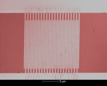 |
| Colorized micrograph of an ultrafast single-photon detector made of superconducting nanowires. NIST researchers use electron beam lithography to pattern the nanowires (vertical lines) on a thin film of tungsten-silicon alloy, which produces more reliable signals than the niobium nitride material used previously. Credit: Baek/NIST |
Abstract:
By swapping one superconducting material for another, researchers at the National Institute of Standards and Technology (NIST) have found a practical way to boost the efficiency of the world's fastest single-photon detector, while also extending light sensitivity to longer wavelengths. The new tungsten-silicon alloy could make the ultrafast detectors more practical for use in quantum communications and computing systems, experiments testing the nature of reality, and emerging applications such as remote sensing.
Key Ingredient: Change in Material Boosts Prospects of Ultrafast Single-photon Detector
Boulder, CO | Posted on July 2nd, 2011The detector, made of superconducting nanowires, is one of several sensor designs developed or used at NIST to register individual photons (particles of light). The original nanowire detector, invented in Russia, uses wires made of niobium nitride and has a detection or quantum efficiency�ability to generate an electrical signal for each arriving photon�of less than 10 percent in its simplest, most compact model. NIST's tungsten-silicon alloy version has an efficiency of 19 to 40 percent over a broad wavelength range of 1280 to 1650 nanometers, including bands used in telecommunications.* The limitations are due mainly to imperfect photon absorption, suggesting that, with further design improvements, detector efficiency could approach 100 percent reliably, researchers say.
Superconducting nanowire detectors have many advantages. They are very fast, able to count nearly a billion photons per second, and they operate over a large range of wavelengths, have low dark (false) counts, and produce strong signals, especially at telecom wavelengths. The detectors produce a signal when a photon breaks apart some of the electron pairs that carry current in the superconducting state, where the material has zero resistance. If the nanowires are narrow enough and the DC current across the device is very close to the transition between ordinary and super conductance, a resistive band temporarily forms across each wire, resulting in a measurable voltage pulse.
Niobium nitride is difficult to make into nanowires that are narrow, long, and sensitive enough to work well. NIST researchers selected the tungsten-silicon alloy mainly because it has higher energy sensitivity, resulting in more reliable signals. A photon breaks more electron pairs in the tungsten-silicon alloy than in niobium nitride. The tungsten alloy also has a more uniform and less granular internal structure, making the nanowires more reliably sensitive throughout. As a result of the higher energy sensitivity, tungsten-silicon nanowires can have larger dimensions (150 nanometers wide versus 100 nanometers or less for niobium nitride), which enlarges the detectors' functional areas to more easily capture all photons.
The NIST team now hopes to raise the efficiency of tungsten alloy detectors by embedding them in optical cavities, which trap light for extremely high absorption. High efficiency may enable the use of nanowire detectors in demanding applications such as linear optical quantum computing, which encodes information in single photons. An equally intriguing application may be an experiment to test quantum mechanics�the so-called "loophole-free Bell test." This test of what Einstein called "spooky action at a distance" depends critically on having a nearly 100-percent efficient photon detector. Tungsten-silicon detectors also are sensitive to longer wavelengths of light, in the mid-infrared range, which could be useful for applications such as laser-based remote sensing of trace gases.
* B. Baek, A.E. Lita, V. Verma and S.W. Nam. Superconducting a-WxSi1-x nanowire single-photon detector with saturated internal quantum efficiency from visible to 1850 nm. Applied Physics Letters 98, 251105. Published online June 21, 2011.
####
About National Institute of Standards and Technology (NIST)
The National Institute of Standards and Technology (NIST) is an agency of the U.S. Department of Commerce.
For more information, please click here
Contacts:
Laura Ost
303-497-4880
Copyright © NIST
If you have a comment, please Contact us.Issuers of news releases, not 7th Wave, Inc. or Nanotechnology Now, are solely responsible for the accuracy of the content.
Bookmark:


| Related News Press |
News and information
![]() Simulating magnetization in a Heisenberg quantum spin chain April 5th, 2024
Simulating magnetization in a Heisenberg quantum spin chain April 5th, 2024
![]() NRL charters Navy�s quantum inertial navigation path to reduce drift April 5th, 2024
NRL charters Navy�s quantum inertial navigation path to reduce drift April 5th, 2024
![]() Discovery points path to flash-like memory for storing qubits: Rice find could hasten development of nonvolatile quantum memory April 5th, 2024
Discovery points path to flash-like memory for storing qubits: Rice find could hasten development of nonvolatile quantum memory April 5th, 2024
Laboratories
![]() A battery�s hopping ions remember where they�ve been: Seen in atomic detail, the seemingly smooth flow of ions through a battery�s electrolyte is surprisingly complicated February 16th, 2024
A battery�s hopping ions remember where they�ve been: Seen in atomic detail, the seemingly smooth flow of ions through a battery�s electrolyte is surprisingly complicated February 16th, 2024
![]() NRL discovers two-dimensional waveguides February 16th, 2024
NRL discovers two-dimensional waveguides February 16th, 2024
![]() Three-pronged approach discerns qualities of quantum spin liquids November 17th, 2023
Three-pronged approach discerns qualities of quantum spin liquids November 17th, 2023
Govt.-Legislation/Regulation/Funding/Policy
![]() NRL charters Navy�s quantum inertial navigation path to reduce drift April 5th, 2024
NRL charters Navy�s quantum inertial navigation path to reduce drift April 5th, 2024
![]() Discovery points path to flash-like memory for storing qubits: Rice find could hasten development of nonvolatile quantum memory April 5th, 2024
Discovery points path to flash-like memory for storing qubits: Rice find could hasten development of nonvolatile quantum memory April 5th, 2024
![]() Chemical reactions can scramble quantum information as well as black holes April 5th, 2024
Chemical reactions can scramble quantum information as well as black holes April 5th, 2024
Quantum Computing
![]() Simulating magnetization in a Heisenberg quantum spin chain April 5th, 2024
Simulating magnetization in a Heisenberg quantum spin chain April 5th, 2024
![]() Discovery points path to flash-like memory for storing qubits: Rice find could hasten development of nonvolatile quantum memory April 5th, 2024
Discovery points path to flash-like memory for storing qubits: Rice find could hasten development of nonvolatile quantum memory April 5th, 2024
![]() With VECSELs towards the quantum internet Fraunhofer: IAF achieves record output power with VECSEL for quantum frequency converters April 5th, 2024
With VECSELs towards the quantum internet Fraunhofer: IAF achieves record output power with VECSEL for quantum frequency converters April 5th, 2024
![]() Chemical reactions can scramble quantum information as well as black holes April 5th, 2024
Chemical reactions can scramble quantum information as well as black holes April 5th, 2024
Sensors
Discoveries
![]() Chemical reactions can scramble quantum information as well as black holes April 5th, 2024
Chemical reactions can scramble quantum information as well as black holes April 5th, 2024
![]() New micromaterial releases nanoparticles that selectively destroy cancer cells April 5th, 2024
New micromaterial releases nanoparticles that selectively destroy cancer cells April 5th, 2024
![]() Utilizing palladium for addressing contact issues of buried oxide thin film transistors April 5th, 2024
Utilizing palladium for addressing contact issues of buried oxide thin film transistors April 5th, 2024
Announcements
![]() NRL charters Navy�s quantum inertial navigation path to reduce drift April 5th, 2024
NRL charters Navy�s quantum inertial navigation path to reduce drift April 5th, 2024
![]() Discovery points path to flash-like memory for storing qubits: Rice find could hasten development of nonvolatile quantum memory April 5th, 2024
Discovery points path to flash-like memory for storing qubits: Rice find could hasten development of nonvolatile quantum memory April 5th, 2024
Tools
![]() Ferroelectrically modulate the Fermi level of graphene oxide to enhance SERS response November 3rd, 2023
Ferroelectrically modulate the Fermi level of graphene oxide to enhance SERS response November 3rd, 2023
![]() The USTC realizes In situ electron paramagnetic resonance spectroscopy using single nanodiamond sensors November 3rd, 2023
The USTC realizes In situ electron paramagnetic resonance spectroscopy using single nanodiamond sensors November 3rd, 2023
|
|
||
|
|
||
| The latest news from around the world, FREE | ||
|
|
||
|
|
||
| Premium Products | ||
|
|
||
|
Only the news you want to read!
Learn More |
||
|
|
||
|
Full-service, expert consulting
Learn More |
||
|
|
||