Home > Press > Layer upon layer: Method holds promise for making two- or three-tier graphene films that could be used for new electronic devices
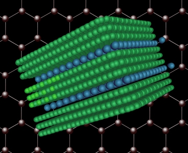 |
| When compounds of bromine or chlorine (represented in blue) are introduced into a block of graphite (shown in green), the atoms find their way into the structure in between every third sheet, thus increasing the spacing between those sheets and making it easier to split them apart. Image: Chih-Jen Shih/Christine Daniloff |
Abstract:
Graphene, a form of pure carbon arranged in a lattice just one atom thick, has interested countless researchers with its unique strength and its electrical and thermal conductivity. But one key property it lacks — which would make it suitable for a plethora of new uses — is the ability to form a band gap, needed for devices such as transistors, computer chips and solar cells.
Layer upon layer: Method holds promise for making two- or three-tier graphene films that could be used for new electronic devices
Cambridge, MA | Posted on June 29th, 2011Now, a team of MIT scientists has found a way to produce graphene in significant quantities in a two- or three-layer form. When the layers are arranged just right, these structures give graphene the much-desired band gap — an energy range that falls between the bands, or energy levels, where electrons can exist in a given material.
"It's a breakthrough in graphene technology," says Michael Strano, the Charles and Hilda Roddey Associate Professor of Chemical Engineering at MIT. The new work is described in a paper published this week in the journal Nature Nanotechnology, co-authored by graduate student Chih-Jen Shih, Professor of Chemical Engineering Daniel Blankschtein, Strano and 10 other students and postdocs.
Graphene was first proven to exist in 2004 (a feat that led to the 2010 Nobel Prize in physics), but making it in quantities large enough for anything but small-scale laboratory research has been a challenge. The standard method remains using adhesive tape to pick up tiny flakes of graphene from a block of highly purified graphite (the material of pencil lead) — a technique that does not lend itself to commercial-scale production.
The new method, however, can be carried out at a scale that opens up the possibility of real, practical applications, Strano says, and makes it possible to produce the precise arrangement of the layers — called A-B stacked, with the atoms in one layer centered over the spaces between atoms in the next — that yields desirable electronic properties.
"If you want a whole lot of bilayers that are A-B stacked, this is the only way to do it," he says.
The trick takes advantage of a technique originally developed as far back as the 1950s and '60s by MIT Institute Professor Mildred Dresselhaus, among others: Compounds of bromine or chlorine introduced into a block of graphite naturally find their way into the structure of the material, inserting themselves regularly between every other layer, or in some cases every third layer, and pushing the layers slightly farther apart in the process. Strano and his team found that when the graphite is dissolved, it naturally comes apart where the added atoms lie, forming graphene flakes two or three layers thick.
"Because this dispersion process can be very gentle, we end up with much larger flakes" than anyone has made using other methods, Strano says. "Graphene is a very fragile material, so it requires gentle processing."
Such formations are "one of the most promising candidates for post-silicon nanoelectronics," the authors say in their paper. The flakes produced by this method, as large as 50 square micrometers in area, are large enough to be useful for electronic applications, they say. To prove the point, they were able to manufacture some simple transistors on the material.
The material can now be used to explore the development of new kinds of electronic and optoelectronic devices, Strano says. And unlike the "Scotch tape" approach to making graphene, "our approach is industrially relevant," Strano says.
James Tour, a professor of chemistry and of mechanical engineering and materials science at Rice University, who was not involved in this research, says the work involved "brilliant experiments" that produced convincing statistics. He added that further work would be needed to improve the yield of usable graphene material in their solutions, now at about 35 to 40 percent, to more than 90 percent. But once that is achieved, he says, "this solution-phase method could dramatically lower the cost of these unique materials and speed the commercialization of them in applications such as optical electronics and conductive composites."
While it's hard to predict how long it will take to develop this method to the point of commercial applications, Strano says, "it's coming about at a breakneck pace." A similar solvent-based method for making single-layer graphene is already being used to manufacture some flat-screen television sets, and "this is definitely a big step" toward making bilayer or trilayer devices, he says.
The work was supported by grants from the U.S. Office of Naval Research through a multi-university initiative that includes Harvard University and Boston University along with MIT, as well as from the Dupont/MIT Alliance, a David H. Koch fellowship, and the Army Research Office through the Institute for Soldier Nanotechnologies at MIT.
####
For more information, please click here
Contacts:
77 Massachusetts Avenue, Room 11-400
Cambridge, MA 02139-4307
617.253.2700
TTY 617.258.9344
Copyright © MIT
If you have a comment, please Contact us.Issuers of news releases, not 7th Wave, Inc. or Nanotechnology Now, are solely responsible for the accuracy of the content.
Bookmark:


| Related News Press |
News and information
![]() Simulating magnetization in a Heisenberg quantum spin chain April 5th, 2024
Simulating magnetization in a Heisenberg quantum spin chain April 5th, 2024
![]() NRL charters Navy’s quantum inertial navigation path to reduce drift April 5th, 2024
NRL charters Navy’s quantum inertial navigation path to reduce drift April 5th, 2024
![]() Discovery points path to flash-like memory for storing qubits: Rice find could hasten development of nonvolatile quantum memory April 5th, 2024
Discovery points path to flash-like memory for storing qubits: Rice find could hasten development of nonvolatile quantum memory April 5th, 2024
Graphene/ Graphite
![]() NRL discovers two-dimensional waveguides February 16th, 2024
NRL discovers two-dimensional waveguides February 16th, 2024
Govt.-Legislation/Regulation/Funding/Policy
![]() NRL charters Navy’s quantum inertial navigation path to reduce drift April 5th, 2024
NRL charters Navy’s quantum inertial navigation path to reduce drift April 5th, 2024
![]() Discovery points path to flash-like memory for storing qubits: Rice find could hasten development of nonvolatile quantum memory April 5th, 2024
Discovery points path to flash-like memory for storing qubits: Rice find could hasten development of nonvolatile quantum memory April 5th, 2024
![]() Chemical reactions can scramble quantum information as well as black holes April 5th, 2024
Chemical reactions can scramble quantum information as well as black holes April 5th, 2024
Chip Technology
![]() Discovery points path to flash-like memory for storing qubits: Rice find could hasten development of nonvolatile quantum memory April 5th, 2024
Discovery points path to flash-like memory for storing qubits: Rice find could hasten development of nonvolatile quantum memory April 5th, 2024
![]() Utilizing palladium for addressing contact issues of buried oxide thin film transistors April 5th, 2024
Utilizing palladium for addressing contact issues of buried oxide thin film transistors April 5th, 2024
![]() HKUST researchers develop new integration technique for efficient coupling of III-V and silicon February 16th, 2024
HKUST researchers develop new integration technique for efficient coupling of III-V and silicon February 16th, 2024
Discoveries
![]() Chemical reactions can scramble quantum information as well as black holes April 5th, 2024
Chemical reactions can scramble quantum information as well as black holes April 5th, 2024
![]() New micromaterial releases nanoparticles that selectively destroy cancer cells April 5th, 2024
New micromaterial releases nanoparticles that selectively destroy cancer cells April 5th, 2024
![]() Utilizing palladium for addressing contact issues of buried oxide thin film transistors April 5th, 2024
Utilizing palladium for addressing contact issues of buried oxide thin film transistors April 5th, 2024
Announcements
![]() NRL charters Navy’s quantum inertial navigation path to reduce drift April 5th, 2024
NRL charters Navy’s quantum inertial navigation path to reduce drift April 5th, 2024
![]() Discovery points path to flash-like memory for storing qubits: Rice find could hasten development of nonvolatile quantum memory April 5th, 2024
Discovery points path to flash-like memory for storing qubits: Rice find could hasten development of nonvolatile quantum memory April 5th, 2024
Military
![]() NRL charters Navy’s quantum inertial navigation path to reduce drift April 5th, 2024
NRL charters Navy’s quantum inertial navigation path to reduce drift April 5th, 2024
![]() What heat can tell us about battery chemistry: using the Peltier effect to study lithium-ion cells March 8th, 2024
What heat can tell us about battery chemistry: using the Peltier effect to study lithium-ion cells March 8th, 2024
![]() New chip opens door to AI computing at light speed February 16th, 2024
New chip opens door to AI computing at light speed February 16th, 2024
Energy
![]() Development of zinc oxide nanopagoda array photoelectrode: photoelectrochemical water-splitting hydrogen production January 12th, 2024
Development of zinc oxide nanopagoda array photoelectrode: photoelectrochemical water-splitting hydrogen production January 12th, 2024
![]() Shedding light on unique conduction mechanisms in a new type of perovskite oxide November 17th, 2023
Shedding light on unique conduction mechanisms in a new type of perovskite oxide November 17th, 2023
![]() Inverted perovskite solar cell breaks 25% efficiency record: Researchers improve cell efficiency using a combination of molecules to address different November 17th, 2023
Inverted perovskite solar cell breaks 25% efficiency record: Researchers improve cell efficiency using a combination of molecules to address different November 17th, 2023
![]() The efficient perovskite cells with a structured anti-reflective layer – another step towards commercialization on a wider scale October 6th, 2023
The efficient perovskite cells with a structured anti-reflective layer – another step towards commercialization on a wider scale October 6th, 2023
Grants/Sponsored Research/Awards/Scholarships/Gifts/Contests/Honors/Records
![]() Discovery points path to flash-like memory for storing qubits: Rice find could hasten development of nonvolatile quantum memory April 5th, 2024
Discovery points path to flash-like memory for storing qubits: Rice find could hasten development of nonvolatile quantum memory April 5th, 2024
![]() Chemical reactions can scramble quantum information as well as black holes April 5th, 2024
Chemical reactions can scramble quantum information as well as black holes April 5th, 2024
Research partnerships
![]() Discovery points path to flash-like memory for storing qubits: Rice find could hasten development of nonvolatile quantum memory April 5th, 2024
Discovery points path to flash-like memory for storing qubits: Rice find could hasten development of nonvolatile quantum memory April 5th, 2024
![]() Researchers’ approach may protect quantum computers from attacks March 8th, 2024
Researchers’ approach may protect quantum computers from attacks March 8th, 2024
![]() 'Sudden death' of quantum fluctuations defies current theories of superconductivity: Study challenges the conventional wisdom of superconducting quantum transitions January 12th, 2024
'Sudden death' of quantum fluctuations defies current theories of superconductivity: Study challenges the conventional wisdom of superconducting quantum transitions January 12th, 2024
Solar/Photovoltaic
![]() Development of zinc oxide nanopagoda array photoelectrode: photoelectrochemical water-splitting hydrogen production January 12th, 2024
Development of zinc oxide nanopagoda array photoelectrode: photoelectrochemical water-splitting hydrogen production January 12th, 2024
![]() Shedding light on unique conduction mechanisms in a new type of perovskite oxide November 17th, 2023
Shedding light on unique conduction mechanisms in a new type of perovskite oxide November 17th, 2023
![]() Inverted perovskite solar cell breaks 25% efficiency record: Researchers improve cell efficiency using a combination of molecules to address different November 17th, 2023
Inverted perovskite solar cell breaks 25% efficiency record: Researchers improve cell efficiency using a combination of molecules to address different November 17th, 2023
![]() Charged “molecular beasts” the basis for new compounds: Researchers at Leipzig University use “aggressive” fragments of molecular ions for chemical synthesis November 3rd, 2023
Charged “molecular beasts” the basis for new compounds: Researchers at Leipzig University use “aggressive” fragments of molecular ions for chemical synthesis November 3rd, 2023
|
|
||
|
|
||
| The latest news from around the world, FREE | ||
|
|
||
|
|
||
| Premium Products | ||
|
|
||
|
Only the news you want to read!
Learn More |
||
|
|
||
|
Full-service, expert consulting
Learn More |
||
|
|
||