Home > Press > Periodic structures in organic light-emitters can efficiently enhance and replenish surface plasmon waves
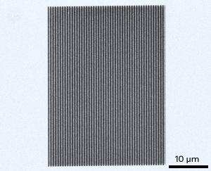 |
| A scanning electron microscope image of an organic grating used to excite surface plasmons |
Abstract:
The irradiation of a metal surface with light or electrons can result in the formation of coherent electronic oscillations called surface plasmons, an effect ideal for applications such as optical communications on optoelectronic chips. Unfortunately, however, surface plasmons quickly lose their energy during transit, limiting their on-chip propagation distance. Jing Hua Teng at the A*STAR Institute of Materials Research and Engineering and co-workers from Nankai University and Nanyang Technological University under the Singapore-China Joint Research Program have now developed nanoscale structures that are able to replenish as well as guide surface plasmons on chips[1]. "These structures can be used as plasmonic sources for lab-on-a-chip applications," says Teng.
Periodic structures in organic light-emitters can efficiently enhance and replenish surface plasmon waves
Singapore | Posted on June 9th, 2011At the resonance frequency, surface plasmons can generate intense light fields close to the surface, especially in metallic nanostructures. For this reason, surface plasmons have been widely studied for a variety of sensing and light-focusing applications. However, the electrical resistance of metals inevitably causes losses in the movements of the electronic currents involved in surface plasmons. It is therefore important to develop schemes that are able to regenerate surface plasmons as they travel along the surface of a chip.
One possibility is the use of organic light-emitting molecules such as rhodamine B. The researchers embedded molecules of rhodamine B in a polymer matrix that was then poured onto the surface of a silver film. To couple the light emission from rhodamine B to the surface plasmons, the polymer layer was structured into a periodic grating (pictured) matched to the resonance frequency of the plasmons. Adjusting the shape and periodicity of the grating allows the light emitted from the surface plasmons to be tailored.
Similar gratings are also used as mirrors in conventional on-chip semiconductor lasers. This structural similarity raises the possibility of combining the plasmonic effects demonstrated here with existing laser designs�an approach that could well lead to the realization of a plasmonic laser.
The advantage of a plasmonic laser over a semiconductor laser is that it can be made much smaller, which is important for the miniaturization of photonic circuits and on-chip sensing applications. "However, such lasers are difficult to fabricate," says Teng. "A number of challenges remain, including how to sufficiently confine the surface plasmons between the mirrors in this kind of configuration and how to reduce the metal damping losses."
Whether for applications in sensing or the on-chip manipulation of light, the potential of these gratings for replenishing plasmons represents an important step toward making plasmonics the key technology for photonic applications in nanoscience.
The A*STAR-affiliated researchers contributing to this research are from the Institute of Materials Research and Engineering
Journal information
[1] Zhang, D. G., Yuan, X. C. & Teng, J. H. Surface plasmon-coupled emission on metallic film coated with dye-doped polymer nanogratings. Applied Physics Letters 97, 231117 (2010).
####
For more information, please click here
Contacts:
Lee Swee Heng
Copyright © The Agency for Science, Technology and Research (A*STAR)
If you have a comment, please Contact us.Issuers of news releases, not 7th Wave, Inc. or Nanotechnology Now, are solely responsible for the accuracy of the content.
Bookmark:


| Related Links |
| Related News Press |
News and information
![]() Simulating magnetization in a Heisenberg quantum spin chain April 5th, 2024
Simulating magnetization in a Heisenberg quantum spin chain April 5th, 2024
![]() NRL charters Navy�s quantum inertial navigation path to reduce drift April 5th, 2024
NRL charters Navy�s quantum inertial navigation path to reduce drift April 5th, 2024
![]() Discovery points path to flash-like memory for storing qubits: Rice find could hasten development of nonvolatile quantum memory April 5th, 2024
Discovery points path to flash-like memory for storing qubits: Rice find could hasten development of nonvolatile quantum memory April 5th, 2024
![]() Good as gold - improving infectious disease testing with gold nanoparticles April 5th, 2024
Good as gold - improving infectious disease testing with gold nanoparticles April 5th, 2024
Display technology/LEDs/SS Lighting/OLEDs
![]() Utilizing palladium for addressing contact issues of buried oxide thin film transistors April 5th, 2024
Utilizing palladium for addressing contact issues of buried oxide thin film transistors April 5th, 2024
![]() Light guide plate based on perovskite nanocomposites November 3rd, 2023
Light guide plate based on perovskite nanocomposites November 3rd, 2023
![]() Simple ballpoint pen can write custom LEDs August 11th, 2023
Simple ballpoint pen can write custom LEDs August 11th, 2023
Lab-on-a-chip
![]() Micro-scale opto-thermo-mechanical actuation in the dry adhesive regime Peer-Reviewed Publication September 24th, 2021
Micro-scale opto-thermo-mechanical actuation in the dry adhesive regime Peer-Reviewed Publication September 24th, 2021
![]() Silicon-graphene hybrid plasmonic waveguide photodetectors beyond 1.55 μm March 13th, 2020
Silicon-graphene hybrid plasmonic waveguide photodetectors beyond 1.55 μm March 13th, 2020
Sensors
Discoveries
![]() Chemical reactions can scramble quantum information as well as black holes April 5th, 2024
Chemical reactions can scramble quantum information as well as black holes April 5th, 2024
![]() New micromaterial releases nanoparticles that selectively destroy cancer cells April 5th, 2024
New micromaterial releases nanoparticles that selectively destroy cancer cells April 5th, 2024
![]() Utilizing palladium for addressing contact issues of buried oxide thin film transistors April 5th, 2024
Utilizing palladium for addressing contact issues of buried oxide thin film transistors April 5th, 2024
Announcements
![]() NRL charters Navy�s quantum inertial navigation path to reduce drift April 5th, 2024
NRL charters Navy�s quantum inertial navigation path to reduce drift April 5th, 2024
![]() Discovery points path to flash-like memory for storing qubits: Rice find could hasten development of nonvolatile quantum memory April 5th, 2024
Discovery points path to flash-like memory for storing qubits: Rice find could hasten development of nonvolatile quantum memory April 5th, 2024
Photonics/Optics/Lasers
![]() With VECSELs towards the quantum internet Fraunhofer: IAF achieves record output power with VECSEL for quantum frequency converters April 5th, 2024
With VECSELs towards the quantum internet Fraunhofer: IAF achieves record output power with VECSEL for quantum frequency converters April 5th, 2024
![]() Nanoscale CL thermometry with lanthanide-doped heavy-metal oxide in TEM March 8th, 2024
Nanoscale CL thermometry with lanthanide-doped heavy-metal oxide in TEM March 8th, 2024
![]() Optically trapped quantum droplets of light can bind together to form macroscopic complexes March 8th, 2024
Optically trapped quantum droplets of light can bind together to form macroscopic complexes March 8th, 2024
![]() HKUST researchers develop new integration technique for efficient coupling of III-V and silicon February 16th, 2024
HKUST researchers develop new integration technique for efficient coupling of III-V and silicon February 16th, 2024
|
|
||
|
|
||
| The latest news from around the world, FREE | ||
|
|
||
|
|
||
| Premium Products | ||
|
|
||
|
Only the news you want to read!
Learn More |
||
|
|
||
|
Full-service, expert consulting
Learn More |
||
|
|
||