Home > Press > Microscopy with a quantum tip
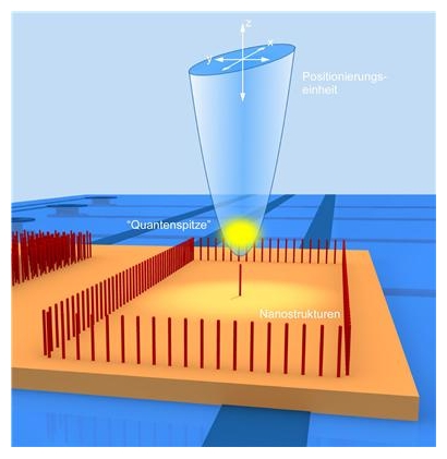 |
| An ultra-cold cloud of atoms (yellow) is trapped in a magnetic trap and scanned across a nanostruc-tured surface. In �contact mode� a loss of atoms from the cloud can be measured, which depends on the surface topography. In the �dynamical mode� the frequency and amplitude of the cloud�s cen-tre-of-mass oscillation changes depending on the surface structure. Both methods allow the surface topography to be imaged. |
Abstract:
Microscopes make tiny objects visible, as their name suggests. However, modern microscopes often do this in a round-about way, not by optically imaging the object with light, but by probing the surface with a fine, needle-like tip. Here, where optical imaging methods reach their limits, scanning probe microscopes can show, by different methods, structures as small as one millionth of a millimetre. With their help, phenomena in the nanoworld become visible and targeted manipulation becomes possible. The heart of a scanning probe microscope is a moveable, suspended tip, which, like the needle on a record player, reacts to small height variations on the surface, and turns these into signals that can be displayed on a computer.
Microscopy with a quantum tip
Germany | Posted on June 8th, 2011T�bingen researchers have now been able to create this tip, not out of solid material, as in the case of the record player, but out of an ultra-cold, dilute gas of atoms. To do this, they cooled an especially pure gas of rubidium atoms to a temperature less than a millionth of a degree above absolute zero temperature, and stored the atoms in a magnetic trap. This "quantum tip" can be precisely positioned and enables the probing of nanostructured surfaces. With this method, more accurate measurements of the interactions between atoms and surfaces are possible and further cooling of the probe tip gives rise to a so-called Bose-Einstein condensate, which allows a significant increase in the resolution of the microscope. The work was led by Prof. Dr. J�zsef Fort�gh, head of the Nano-Atom-Optics group, and his co-worker Dr. Andreas G�nther. PhD student Michael Gierling is first author of the study, which appeared on May 29 as an advance online publication in the scientific journal "Nature Nanotechnology".
The scientists demonstrated the use of their cold-atom scanning probe tip by testing a surface with vertically grown carbon nanotubes. The tip was scanned over the sample using a type of magnetic conveyor belt. The first measurements in the so-called "contact mode" revealed how the tall tubes stripped some atoms out of the atom cloud. These atom losses told the researchers about the location and height of the nanotubes and enabled the imaging of the surface topography.
When the temperature of an atomic gas approaches absolute zero, a quantum mechanical phenomenon occurs, turning the cloud into what's known as a Bose-Einstein condensate. In this state it is no longer possible to distinguish between the atoms. They become, so to speak, a single, giant "super-atom". With such a Bose-Einstein condensate it was possible for the T�bingen scientists to microscopically resolve individual freestanding nanotubes. According to the researchers, future improvements to the cold-atom scanning probe microscope could, in theory, increase the current resolution of about eight micrometres by a factor of a thousand.
The microscope also functions in the so-called "dynamical mode". The researchers again created a Bose-Einstein condensate close to the nanotubes. They then allowed the condensate to oscillate perpendicular to the surface, and observed how the frequency and size of these oscillations changed, depending on the topography of the nanostructured sample. In this way they were able to obtain a well resolved image of the surface. The researchers write that this method has an advantage because no atoms are loss from the cloud. This could be helpful in cases where atoms that are adsorbed on the sample might influence subsequent measurements.
The researchers conclude: "the extreme purity of the probe tip and quantum control over the atomic states in a Bose-Einstein condensate open up new possibilities of scanning probe microscopy with non-classical probe tips". Beyond this, the researchers hope to develop new applications from the demonstrated coupling between ultra-cold quantum gases and nanostructures.
The study was done within the framework of the BMBF programme "NanoFutur" and in collaboration with several groups from the Center for Collective Quantum Phenomena (CQ) T�bingen, to which various research groups from the Faculty of Mathematics and Natural Science belong.
Full bibliographic information
M. Gierling, P. Schneewei�, G. Visanescu, P. Federsel, M. H�ffner, D. P. Kern, T. E. Judd, A. G�n-ther, and J. Fort�gh: Cold-atom scanning probe microscopy. Nature Nanotechnology, Online-publication from 29th May 2011, DOI: 10.1038/NNANO.2011.80
####
For more information, please click here
Contacts:
Michael Seifert
Dr. Andreas G�nther &
Prof. Dr. J�zsef Fort�gh
Universit�t T�bingen
Physikalisches Institut
Arbeitsgruppe Nano-Atomoptik
Telephone: +49 (0) 7071 29 76281
+49 (0) 7071 29 76270
E-mail:
Copyright © AlphaGalileo
If you have a comment, please Contact us.Issuers of news releases, not 7th Wave, Inc. or Nanotechnology Now, are solely responsible for the accuracy of the content.
Bookmark:


| Related News Press |
News and information
![]() Simulating magnetization in a Heisenberg quantum spin chain April 5th, 2024
Simulating magnetization in a Heisenberg quantum spin chain April 5th, 2024
![]() NRL charters Navy�s quantum inertial navigation path to reduce drift April 5th, 2024
NRL charters Navy�s quantum inertial navigation path to reduce drift April 5th, 2024
![]() Discovery points path to flash-like memory for storing qubits: Rice find could hasten development of nonvolatile quantum memory April 5th, 2024
Discovery points path to flash-like memory for storing qubits: Rice find could hasten development of nonvolatile quantum memory April 5th, 2024
Imaging
![]() Nanoscale CL thermometry with lanthanide-doped heavy-metal oxide in TEM March 8th, 2024
Nanoscale CL thermometry with lanthanide-doped heavy-metal oxide in TEM March 8th, 2024
![]() The USTC realizes In situ electron paramagnetic resonance spectroscopy using single nanodiamond sensors November 3rd, 2023
The USTC realizes In situ electron paramagnetic resonance spectroscopy using single nanodiamond sensors November 3rd, 2023
![]() Observation of left and right at nanoscale with optical force October 6th, 2023
Observation of left and right at nanoscale with optical force October 6th, 2023
Discoveries
![]() Chemical reactions can scramble quantum information as well as black holes April 5th, 2024
Chemical reactions can scramble quantum information as well as black holes April 5th, 2024
![]() New micromaterial releases nanoparticles that selectively destroy cancer cells April 5th, 2024
New micromaterial releases nanoparticles that selectively destroy cancer cells April 5th, 2024
![]() Utilizing palladium for addressing contact issues of buried oxide thin film transistors April 5th, 2024
Utilizing palladium for addressing contact issues of buried oxide thin film transistors April 5th, 2024
Announcements
![]() NRL charters Navy�s quantum inertial navigation path to reduce drift April 5th, 2024
NRL charters Navy�s quantum inertial navigation path to reduce drift April 5th, 2024
![]() Discovery points path to flash-like memory for storing qubits: Rice find could hasten development of nonvolatile quantum memory April 5th, 2024
Discovery points path to flash-like memory for storing qubits: Rice find could hasten development of nonvolatile quantum memory April 5th, 2024
Tools
![]() Ferroelectrically modulate the Fermi level of graphene oxide to enhance SERS response November 3rd, 2023
Ferroelectrically modulate the Fermi level of graphene oxide to enhance SERS response November 3rd, 2023
![]() The USTC realizes In situ electron paramagnetic resonance spectroscopy using single nanodiamond sensors November 3rd, 2023
The USTC realizes In situ electron paramagnetic resonance spectroscopy using single nanodiamond sensors November 3rd, 2023
Photonics/Optics/Lasers
![]() With VECSELs towards the quantum internet Fraunhofer: IAF achieves record output power with VECSEL for quantum frequency converters April 5th, 2024
With VECSELs towards the quantum internet Fraunhofer: IAF achieves record output power with VECSEL for quantum frequency converters April 5th, 2024
![]() Nanoscale CL thermometry with lanthanide-doped heavy-metal oxide in TEM March 8th, 2024
Nanoscale CL thermometry with lanthanide-doped heavy-metal oxide in TEM March 8th, 2024
![]() Optically trapped quantum droplets of light can bind together to form macroscopic complexes March 8th, 2024
Optically trapped quantum droplets of light can bind together to form macroscopic complexes March 8th, 2024
![]() HKUST researchers develop new integration technique for efficient coupling of III-V and silicon February 16th, 2024
HKUST researchers develop new integration technique for efficient coupling of III-V and silicon February 16th, 2024
|
|
||
|
|
||
| The latest news from around the world, FREE | ||
|
|
||
|
|
||
| Premium Products | ||
|
|
||
|
Only the news you want to read!
Learn More |
||
|
|
||
|
Full-service, expert consulting
Learn More |
||
|
|
||